Transistors in computer chips work electrically, but the data can be transmitted more quickly with light. Researchers have therefore been looking for a way to integrate a laser directly into silicon chips for a long time. Researchers at C2N, in collaboration in particular with researchers at Germany’s Forschungszentrum Jülich (FZJ) and STMicroelectronics, have implemented a new material engineering method to fabricate a laser microdisk in strained Germanium-Tin (GeSn) alloy. They demonstrate for the first time the laser device with a group IV compound, compatible with Silicon, operating with ultra-low threshold and under continuous wave excitation.
Optical data transmission enables significantly higher data rates and ranges than conventional electronic processes, and at the same time requires less energy. In data centers, optical cables of a length of around one meter are therefore standard. In the future, optical solutions will be required for shorter distances to transfer data from board to board or chip to chip. An electrically pumped laser that is compatible with silicon-based CMOS technology would be ideal to achieve very high data rates.
Germanium-Tin alloys (GeSn) are promising for realizing light emitters, such as lasers. Based entirely on group IV semiconductor elements, this alloy is compatible with Silicon and can be fully integrated in the CMOS fabrication chain, widely used to produce electronic chips for mainstream applications. Today, the main approach consists in introducing as much tin as possible in the GeSn alloy (in the range of 10-16%). The obtained compound thus provides direct alignment of the band structure, which makes it possible the laser emission. However, this approach has major drawbacks: due to the lattice mismatch between the Germanium (strained relaxed) substrate on silicon and the Sn-rich GeSn alloys, a very dense dislocation defects network is formed at the interface. It thus takes extremely high densities of power pumping (hundreds of kW/cm² at cryogenic temperature) to reach the laser emission regime.
Using a different approach based on specific material engineering, a team composed of researchers at C2N, at the Forschungszentrum Jülich (FZJ Germany) and at STMicroelectronics, has obtained a laser emission in a microdisk of GeSn alloy fully encapsulated by a stressor layermade of dielectric Silicon Nitride (SiNx). With this device, they have demonstrated for the first time the laser emission in the alloy able to operate under continuous-wave (cw) excitation. Laser effect is reached under cw and pulsed excitations, with ultra-low thresholds compared to the current state of the art. Their results are published in Nature Photonics.
This device uses a 300 nm thick GeSn layer with a tin content as low as 5.4% which was encapsulated by a SiNx stressor layer to produce a tensile strain of the lattice. The as-grown alloy layer is initially an indirect band-gap semiconductor that does not support laser effect and is a very poor emitter. Researchers evidenced that it can be transformed into a truly direct band-gap semiconductor that can support laser effect, and thus becomes an efficient emitter by applying the tensile strain to it. Additionally the tensile strain delivers a low density of states at the valence band edge, which is the light hole band thus enabling to reduce required excitation level to reach laser action. Thanks to the low concentration of tin, the dislocation networks is less dense and can be more easily treated. A specific1 microdisk cavity design was developed to allow high strain transfer from the stressor layer to the active region, remove the interface defects, and enhanced thermal cooling of the active region.
With this device, the researchers demonstrate for the first time continuous wave (cw) lasing up to 70 K, while pulsed lasing is reached at temperatures up to 100 K. Lasers operating at a wavelength of 2.5 μm have ultra-reduced thresholds of 0.8 kW/cm2 for nanosecond-pulsed optical excitation, and 1.1 kW/cm2 under cw optical excitation. Since these thresholds are 2 order of magnitude lower than reported in the literature, the results open a new path towards the integration of group IV laser on a Si-photonic platform.
1 Patent PCT/FR2017/052881 “Structure comprising a semiconductor strained layer on a heat sink”
- Read about it on the website of Université Paris-Saclay: Demonstration of a continuous laser beam with germanium-tin alloy
- Read about it on the website of the Germany's Forschungszentrum Jülich: High-Efficiency Laser for Silicon Chips
Reference:
Ultra-low-threshold continuous-wave and pulsed lasing in tensile-strained GeSn alloys
Anas Elbaz1,2, Dan Buca3, Nils von den Driesch3,4, Konstantinos Pantzas1, Gilles Patriarche1, Nicolas Zerounian1, Etienne Herth1, Xavier Checoury1, Sebastien Sauvage1, Isabelle Sagnes1, Antonino Foti5, Razvigor Ossikovski5, Jean-Michel Hartmann6, Frederic Boeuf2, Zoran Ikonic7, Philippe Boucaud8, Detlev Grutzmacher3,4, & Moustafa El Kurdi1
Nature Photonics (2020)
DOI : https://doi.org/10.1038/s41566-020-0601-5
1 Centre de Nanosciences et de Nanotechnologies – C2N (CNRS, Université Paris-Saclay), Palaiseau
2 STMicroelectronics, Crolles, France
3 Forschungszentrum Juelich, Germany
4 RWTH Aachen, Germany
5 Laboratoire de Physique des interfaces et couches minces (LPICM), CNRS, Ecole Polytechnique, Université Paris-Saclay, Palaiseau, France
6 CEA, LETI and Univ. Grenoble Alpes, France
7 University of Leeds, UK
8 CRHEA, Université Côte d’Azur, CNRS, Valbonne, France
Contact:
- Moustafa El Kurdi, Associate Professor at Université Paris-Saclay and researcher at C2N
- Dan Buca, Forschungszentrum Juelich (FZJ)
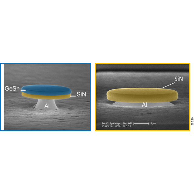
Figure: Scanning Electron Micrographs: (left) A layer of GeSn is transferred onto a silicon substrate and then structured as a microdisk to form an optical cavity. During transfer, the defective layer in the GeSn, which was at the interface with the Ge/Si substrate, was removed by etching. The transfer also makes it possible to insert a stressed SiNx layer underneath the GeSn layer. An Aluminum layer was used to maintain the cavity while allowing excellent thermal cooling of the laser device trough the substrate. (right) A final conformal deposition of a strained film on the microdisk allows to obtain an "all-around" configuration of the stress transfer from the SiNx to the GeSn. The GeSn is then under a tensile strain of 1.6% very homogeneously distributed in its active volume. Credit: C2N / M. El Kurdi & al.