Researchers at the Centre de Nanosciences et de Nanotechnologies (C2N), in collaboration with Laboratoire Interdisciplinaire Carnot de Bourgogne (ICB) have demonstrated the generation of a non-diffractive guided-wave optical beam over a long distance. The exploited concept of Bessel beam, based on the use of a lens with conical surface formed by a 2D array of integrated plasmonic nanoresonators, can be easily adapted to other spectral domains.
Diffraction of electromagnetic waves in 2D or 3D unbounded media and which do not exert any confinement transverse to the propagation direction is one of the worst impairments for application to data transmission in the radio-wave, micro-wave or infrared domains. To counteract this issue, one solution is to shape the intensity profile of the beam with Bessel-like functions, leading to a beam that propagates without being diffracted or spread out. To this end, an axicon-type lens, based on a conical surface, can be used to generate an annular light distribution which remains laterally constant along the optical axis during propagation on a certain distance. Though most efforts devoted to the study of propagation of non-diffractive beams are focused on free space optical applications, the concept could also be useful for planar guided-wave optics to insure propagation of collimated beams over a long distance. The conventional approach relies on self-collimation properties that can be obtained using 2D photonic crystal (PhC) structures. However, its application is essentially limited to the propagation of single lobe Gaussian beams and is not suited for the implementation of Bessel type beam intensity profiles.
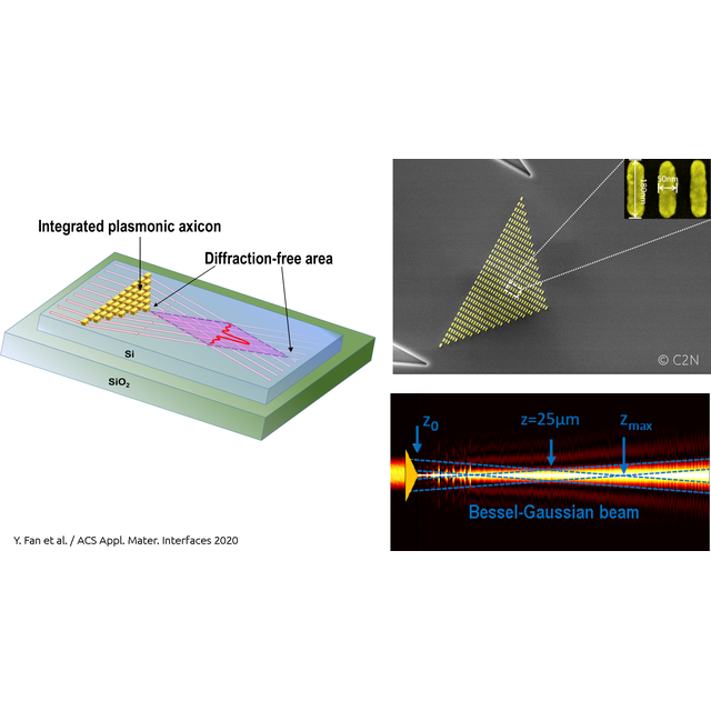
In a work published in April 2020 in ACS Applied Materials & Interfaces journal, a team of researchers at the Photonics Department of the Centre de Nanosciences et de Nanotechnologies – C2N (CNRS/Univ. Paris-Saclay) in collaboration with the Laboratoire Interdisciplinaire Carnot de Bourgogne – ICB (CNRS/Univ. de Bourgogne/Univ. de Technologie Belfort-Montbeliard), presented a new strategy for the generation of a guided-wave Bessellian beam. To attain this objective, they used an integrated dielectric waveguide metasurface axicon lens with a footprint as small as 11µm². The control of the lightwave local phase and amplitude is achieved by adjusting the parameters of such hybrid metasurface-dielectric waveguide, namely the force of the evanescent coupling with plasmonic nanoresonators, their surface density, resonance frequency and quality factor.
The design, modeling and fabrication of the experimental structure, a Bessel beam generator formed by a 2D array of plasmonic nanoresonators integrated on an SOI waveguide (see Figure), were performed at C2N* while the beam propagation measurements were carried out by ICB partners. Near-field scanning optical microscopy technique was used to provide direct evidence of long-range propagation without diffraction of a planar guided beam and to determine its intensity profile. The results presented demonstrate the ability to control the light flux in guided wave structures by locally engineering the effective index by means of a thin metasurface over it. The wide variety of physical parameters that can be used to control the properties of plasmonic resonators offers the possibility of designing nanotechnology-based optical devices with advanced functionalities. The additive character of this generic technology makes it suitable to a wide variety of platforms, such as planar silica, silicon nitride, lithium niobate, II-VI, III-V, IV-IV semiconductors, and so forth.
The exploited concept can also be easily adapted to other spectral domains, especially for longer wavelengths, from mid- and far infrared to THz where the absorption losses of plasmonic resonators are greatly reduced. The sensitivity of the resonant frequency of localized surface plasmons to changes in their dielectric environment can be used for a multitude of applications in environmental and biochemical sensing, defense, security and medicine.
*In the C2N Technology Facility (cleanroom), member of the French network of large high-end facilities (RENATECH CNRS)
References:
2D Waveguided Bessel Beam Generated Using Integrated Metasurface-Based Plasmonic Axicon*
Yulong Fan1, Benoît Cluzel2, Marlène Petit2, Xavier Le Roux1, Anatole Lupu1, Andre de Lustrac1
ACS Appl. Mater. Interfaces (2020)
DOI : doi.org/10.1021/acsami.0c03420
*you can contact Anatole Lupu or André de Lustrac (emails below) to obtain a link to download the full electronic version of the article: up to 50 copies are available for free on the ACS Articles website.
1 Centre de Nanosciences et de Nanotechnologies - C2N (CNRS, Université Paris-Saclay)
2 Laboratoire Interdisciplinaire Carnot de Bourgogne - ICB (CNRS - Université de Bourgogne – Université de Technologie de Belfort-Montbeliard)
Contacts:
- Yulong Fan, C2N Alumni, currently at the City University of Hong Kong
- Benoît Cluzel, Associate Professor at Université de Bourgogne, Researcher at ICB
- Xavier Le Roux, CNRS research engineer at C2N
- Anatole Lupu, CNRS researcher at C2N
- André de Lustrac, Professor Emeritus at C2N
Figure: (Left) Schematic of Bessel beam generator formed by a 2D array of plasmonic nanoresonators integrated on an SOI (Silicon on Insulator) waveguide; (Top right) SEM (scanning electron microscope) image of the fabricated meta-axicon and magnified view of the gold nanoresonators; (Bottom right) SNOM (scanning near-field optical microscope) image of the evolution with propagation distance of the Bessel-Gaussian beam.