News (in French) from Institut des sciences de l'ingénierie et des systèmes (INSIS) of CNRS - 15 october 2018
Mid-infrared (mid-IR) spectroscopy is a nearly universal way to identify chemical and biological substances. Researchers from the Centre de nanosciences et de nanotechnologies and from Politecnico di Milano have developed photonic integrated circuits in the mid-infrared, based on silicon-germanium waveguides. These structures make it possible to achieve integrated sensors capable of detecting concentrations of a few hundred ppm. This work is published in Optical Materials Express.
In the spectral range of the mid-infrared, spectroscopy makes it possible to efficiently identify and quantify different chemical and biological substances. Its exploitation in various applications, especially mobile one, requires components compatible with this range of wavelengths. Researchers from the Centre de nanosciences et de nanotechnologies (C2N, CNRS / Université Paris-Sud) and from Politecnico di Milano are developing photonic integrated circuits in the mid-infrared, based on silicon-germanium waveguides (SiGe). They demonstrated for the first time the potential of these structures for integrated sensors.
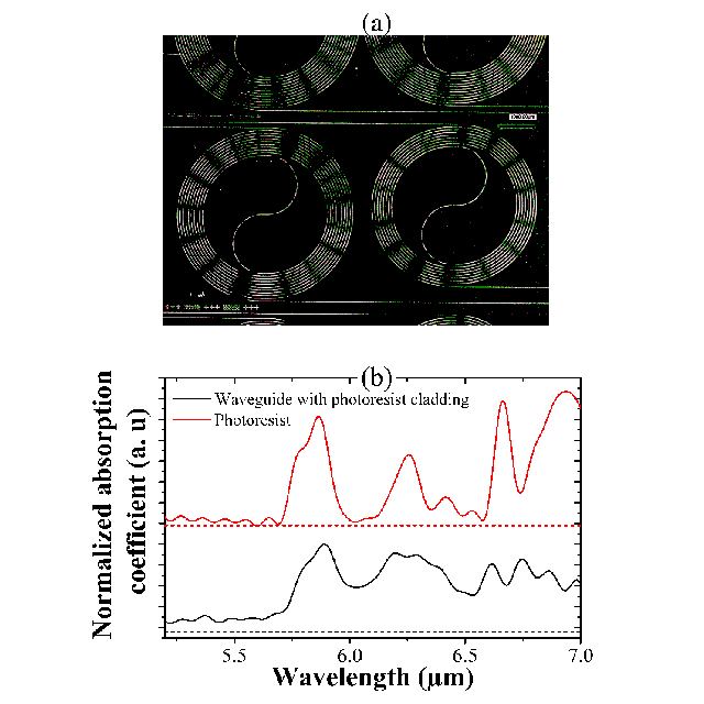
SiGe alloys offer flexible control of the properties of the guide, while taking benefit from the wide transparency of germanium in the mid-infrared. The use of spiral guides increases the surface of interactions while keeping a compact device. The detection takes place with the evanescent part of the optical mode, the part of the wave that propagates along the outer surface of the guide. It thus comes into direct contact with the environment to be analysed. As a first proof of concept, the researchers were able to detect the specific absorption lines between 5.8 and 6.2 μm of a photoresist deposited on the SiGe guides. The results obtained showed that these components should allow the detection of methane at concentrations of a few hundred ppm1, which is lower than the occupational exposure limit recommended by international environmental standards.
This work benefited from the ERC Starting Grant INSPIRE and the C2N platform belonging to the RENATECH2 network.
Notes:
1 ppm : parts per million, 1ppm = 1 mg/kg.
2 RENATECH : French network of academic micro-nano fabrication clean-rooms.
References:
Mid-infrared sensing between 5.2 and 6.6 μm wavelengths using Ge-rich SiGe waveguides,
Q. Liu, J. Manel Ramirez, V. Vakarin, X. Le Roux, A. Ballabio, J. Frigerio, D. Chrastina, G. Isella, D. Bouville, L. Vivien, C. Alonso Ramos, D. Marris-Morini,
Optical Materials Express, 8 (5), 1305 (2018)
DOI : https://doi.org/10.1364/OME.8.001305
Contact: Delphine Marris-Morini, Professor of University Paris-Sud at C2N
Figure: (a) : SiGe spiral waveguides. (b): comparison between the losses of the waveguide covered by the photoresist and the absorption of the photoresist. The absorption peaks of the resin at 5.8 μm; 6.25 and 6.6 μm are clearly visible when measuring waveguide transmission. © C2N – CNRS/UPSUD