A collaboration of researchers from C2N and STMicroelectronics has obtained, for the first time, a laser effect with germanium as active material thanks to direct alignment of the electronic band diagram. Until now, this material was known to be unable to emit light.
Germanium (Ge) belongs to the same family as silicon and is a perfect match for CMOS chip fabrication processes, which are Si-based and low-cost technologies widely used in microelectronics, but also for photonics to achieve integrated optical functions. Nevertheless, the optical source is now the missing block in the development of complex photonic devices using the CMOS environment. So far, neither silicon nor germanium have been able to emit light because of a physical limiting factor: the indirect nature of their band structure.
Thanks to work on the properties of the electronic structure of the Ge, C2N researchers have been able to transform it into a direct bandgap material, allowing the emission of light. To do so, they applied strong tensile strain to the material. They were inspired by CMOS methods, namely the use of films stressor to strain transistor channels and enhance the carrier transport properties. In order to demonstrate a laser, they have revisited this method to strain resonant optical cavities, on much larger volumes than transistors channels. In collaboration with researchers from STMicroelectronics, they were able to obtain for the first time a laser effect with germanium as active material with a direct alignment of the electronic band diagram. Their work has been published in APL Photonics journal. The structure realized consists of microdisks of Ge fully wrapped by a silicon nitride stressor layer. This allowed to reach high level of tensile strain in Ge and to obtain the direct band gap regime. The strained Ge microdisk is sustained by an Aluminium pedestal, which is an excellent heat sink. Thanks to both strain and thermal, management in Ge microdisk cavities, the researchers were able to reach continuous wave laser emission regime under optical pumping.
Researchers at C2N are now working on alloying of Ge with tin, another element of column IV that is compatible with silicon technologies. This would allow to increase the directness of the band structure to boost the device performance and obtain laser effect up to room temperature. This would feed future developments in the field of silicon photonics, especially for the development of active sources.
References:
Germanium microlasers on metallic pedestals,
A. Elbaz1,2, M. El Kurdi1, A. Aassime1, S. Sauvage1, X. Checoury1, I. Sagnes1, C. Baudot2, F. Boeuf2 et P. Boucaud1
APL PHOTONICS (August 2018)
DOI: https://doi.org/10.1063/1.5025705
1 Centre de Nanosciences et de Nanotechnologies – C2N (CNRS / Université Paris-Sud- Université Paris-Saclay)
2 STMicroelectronics, 850 Rue Jean Monnet, F-38920 Grenoble, France
Contact:
- Moustafa El Kurdi, Associate Professor of Université Paris-Sud at C2N
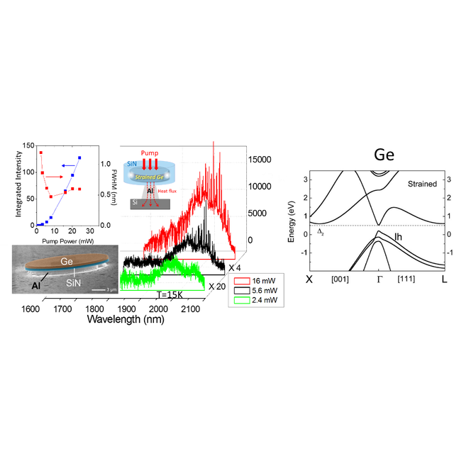
Figure : Left: CW Photoluminescence spectrum of a 12µm diameter strained Ge disk under various incident pump power, water vapor absorption lines modulate the emission below 1940 nm. Resonant mode contribution occurs after a given incident power threshold is reached. The inset gives the integrated intensity and width for a resonant whispering gallery mode as a function of incident power. SEM picture of a Ge disk with a SiN stressor layer at its bottom side and sustained by an Al pedestal. This picture was taken before a final SiN layer deposition. This final SiN deposition allows to realize the ‘’all around stressor’’ structure as shown on the schematic view. Right: electronic band diagram of tensile strained Ge calculated in the framework of a 30-band k.p model. The tensile strain induces a direct alignment of the band structure for biaxial strain as large as 1.7% and above. © C2N/El Kurdi