
Seminars
A new spin on magnetism with applications in information processing
C2N, Amphithéatre, PalaiseauSeminars
Recent advances in magnetism research are likely to have an important impact on electronics and information processing.
These advances use the electron’s magnetic moment (spin) to transmit, change and store information. They enable new devices
that could operate at high speed with very low energy consumption. The information is stored in the orientation of electron magnetic moments in magnetic materials and can persist without power; energy is only needed to change the information. In this talk, I will highlight the new physics concepts and materials that have enabled these advances and discuss some of their applications in information processing.
ATTENTION: subscription for this event is mandatory (on this page : https://framaforms.org/inaugural-lesson-chaires-dalembert-andrew-kent-1542554346).
Probabilistic Aspects of Deterministic Magnetization Dynamics in Single-Domain Nanomagnets
C2N site Palaiseau, Salle A009, PalaiseauSeminars
Single-domain nanomagnets occupy a central position in the research on magnetic phenomena and applications at submicrometer scales, such as coherent magnetization switching, current-induced magnetic torques, and nanomagnet logic. Fundamental as well as application-oriented research in the area of magnetization dynamics this field revolves around the central question: how can one drive a nanomagnet to a prescribed final magnetization state? The simplest answer, which is to apply a sufficiently large magnetic field that destroys all magnetic energy minima except one, is at the core of the classical Stoner- Wohlfarth model. However, this strategy is unsatisfactory in many respects, and the search for more advanced alternatives has become the key issue in recent years, in relation, for example, to precessional or spin-torque-driven magnetization switching. The answer to this question is far from trivial. A striking feature comes from the weakly dissipative nature of magnetization dynamics. In presence of multiple stable states, sensitivity to initial conditions introduces probabilistic aspects in an otherwise purely deterministic dynamics. In the first part of the talk, we introduce these weakly dissipative (quasi-probabilistic) systems by stressing their general nature. Indeed, these systems are encountered in such fields as celestial mechanics, dynamics of charged particles and propagation of electromagnetic waves. We also discuss how the description of this system can be given in terms of Gibbs-type ensembles and the associated phase-flow. In the second part of the talk, we discuss a theoretical analysis of one special case, relevant to magnetic technologies. We demonstrate that in a single-domain nanomagnet, the probability P to relax to one of the two stable equilibrium state can be tuned to any desired value between 0 and 1 by applying a small transverse magnetic field. The transverse field neither breaks the mirror symmetry of the energy function nor introduces any important distortion in the energy profile. Nevertheless, it is enough to alter the effect of the weak dissipative part in a way that drastically modifies the relaxation probabilities. In the last part of the talk we will illustrate the relevance of the presented theory in the problems of field-driven and spin-torque driven precessional (ballistic) switching. Using a combination of analytical and numerical techniques, it is shown that the use of appropriate transverse fields greatly improve the switching reliability. Finally we discuss how the analytical prediction could be exploited to devise novel methods for the measurement of the magnetization damping constant.
*** IMPORTANT ***
Participants external to the C2N laboratory must register using the form below in order to attend the seminar:
https://framaforms.org/registration-c2n-seminar-prof-claudio-serpico-1543975675
Integrated photonics processors for quantum information
C2N, Amphi, Orsay CedexSeminars
Integrated optics platforms are widely explored nowadays for implementing different quantum information protocols and quantum optics experiments, paving routes to quantum technologies. In comparison to their bulk counterparts, on-chip circuits offer advantages in terms of scalability, reconfigurability and phase stability. With this motivation, several on-chip linear optical networks based on different material platforms have been used to implement various quantum optics experiments such as bosonic transport simulations, universal linear optics protocols and so on. In this talk, I will focus on such waveguide devices and our recent work on an 8 x 8 reconfigurable transformation circuit based on single-mode stoichiometric Si3N4 waveguides. The advantage of this platform compared to others is the unique combination of ultra-low straight-propagation loss, spectrally wide transparency range and high index contrast which enables a dense waveguide arrangement. Our preliminary single photon experiments on this device, illustrates strong potential of this platform for quantum information processing protocols.
(in french) Comment compter un photon unique, et trouver un résultat de 1000;et d’autres manips sur la mesure quantique, à l’aide d’atomes froids et des photons intriqués
C2N site Marcoussis, , MarcoussisSeminars
Je présenterai nos travaux expérimentaux concernant les mesures quantiques faites sur des systèmes post-sélectionnés. Notamment, nous nous servons d’atomes froids et de l’effet «EIT» pour créer des interactions photon-photon suffisamment puissantes qu’on observe la phase nonlinéaire imprimée par des impulsions au niveau du photon unique sur un fasiceau sonde. En s’appuyant sur le formalisme de «weak measurement» de Yakir Aharonov et al., nous montrons aussi que quand la mesure est effectuée sur un photon post-sélectionné dans un état final donné, l’effet sur la sonde peut être «amplifié», de sorte qu’une mesure du nombre de photons dans une région d’espace peut même dépasser le nombre de photons total.
Je dirai quelques mots à propos d’autres manips en cours, telle une expérience pour mesurer la durée de la traversée d’une barrière à effet tunnel par les atoms ultrafroids (~900 pK), et une application des idées venues de l’informatique quantique à des problèmes d’imagerie classique (super-résolution).
Controlling Dirac fermions optics in high mobility graphene by scanning gate microscopy
C2N site Marcoussis, Salle R. Planel, MarcoussisSeminars
Abstract:
With the recent progresses in building high mobility graphene samples, new electron optics devices have been envisioned, mostly based on the use of p-n interfaces. At p-n boundaries Dirac fermions behave as would photons encountering a negative index media, therefore experiencing a peculiar refraction known as Veselago lensing. However the lack of tunability of p-n interfaces is an obstacle on the way towards experimental control of Dirac optics. We present a way to create a movable and highly tunable circular Veselago lens in graphene, using the polarized tip of a scanning gate microscope. We image the electron flow through this lens, and observe two points of anti-focusing along transport axis, at a distance from the lens center that depends on the incident particles energy. We explain these features using tight-binding simulations, and show that a circular n-p-n junction induces a low current density away from the junction, interpreted as anti-focusing points. We show that scanning the polarized tip in the vicinity of the constriction allows to map out the behavior of charge carriers around the tip-induced perturbation. Our work paves the way towards a deep understanding of Dirac fermions optical elements, a prerequisite to engineer relativistic electron optics devices.
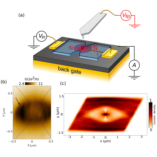
The figure is in attached file, if a caption is needed:
(a) Scheme of the SGM experiment: a polarized tip is scanned above an encapsulated graphene constriction while recording its conductance.
(b) Scanning gate image obtained in a n-p-n configuration. The tip and backgate voltages are chosen to create a circular n-p-n junction. The conductance as a function of this perturbation position is shown, and highlights a spot of high conductance when the tip is at the very center of the constriction, and two spots of reduced conductance when it is placed at both entrances.
(c) Tight binding simulations of the current density around a ciruclar smooth n-p-n junction. Two spots of reduced current density are visible away from the junction, interpreted as anti-focusing points.
Other authors: N. Moreau 1 , S. Somanchi 2 , V.-H. Nguyen 1 , K. Watanabe 3 , T. Taniguchi 3 , J-C. Charlier 1 , C. Stampfer 2 & B. Hackens 1
1 IMCN/NAPS, Université catholique de Louvain, B-1348 Louvain-la-Neuve, Belgium
2 ARA-FIT and 2nd Institute of Physics - RWTH Aachen, Germany
3 National Institute for Materials Science, Namiki, Japan
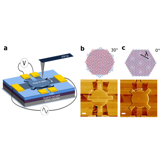
Twistable electronics with dynamically rotatable heterostructures
C2N site Orsay, salle 44, Orsay CedexSeminars
The electronic properties of two-dimensional materials and their heterostructures can be dramatically altered by varying the relative angle between atomic planes. This makes it theoretically possible to realize a new class of twistable electronics in which device properties can be manipulated on-demand by simply rotating the structure. A significant limitation to exploiting this unique degree of freedom, however, has been the difficulty to precisely vary the rotational order. Here, we demonstrate a new device architecture in which a layered heterostructure can be dynamically twisted, in situ. We study graphene encapsulated by boron nitride where at small rotation angles the device characteristics are dominated by coupling to a large wavelength Moir\'e superlattice. The ability to investigate arbitrary rotation angle in a single device reveals new features in the optical, mechanical and electronic response in this system. Our results establish the capability to fabricate twistable electronic devices with dynamically tunable properties.
Si-CMOS-compatible microphotonics platform which will enable on-chip imaging and sensing applications
C2N site Orsay, salle 11, Orsay CedexSeminars
The mid-infrared wavelength range (2.5~12μm) includes the absorption peaks of many important chemicals including environmental and industrial pollutants, toxic agents of interest to homeland security and also the medical drug delivery industry of big pharma. By analyzing the absorption spectrum of a chemical, one can (i) identify the chemical species and (ii) measure its concentration. With a Si CMOS compatible integrated mid-infrared (MIR) platform for sensing, we can envision a network of low-cost sensors for diverse applications. Here I will discuss the main building blocks of an integrated mid-infrared (MIR) sensing platform: the light source, the waveguide sensor and the detector, focusing predominantly on the development of the sensor and detector.
For both, waveguide sensor and photodetector materials, we seek (a) low-cost options with (b) low deposition temperatures for back-end Si-CMOS-compatibility, and (c) robustness against harsh sensing environments. For waveguide sensors to provide good signal to noise ratios, the material must additionally display low absorption and low sidewall scattering losses. Photodetectors must be absorptive at the wavelengths of interest.
We will discuss integration strategies for photodetectors: (i) with a sensor waveguide as well as (ii) with a resonant cavity connectorized to CMOS electronics. The detection of liquids, gases and aerosols using these devices will be discussed. Our work makes us hopeful regarding the future of mid-IR silicon photonic sensor systems.
Speaker bio:
Anu Agarwal
Principal Research Scientist
MIT Materials Research Laboratory
Leader, Lab for Education and Application Prototypes (LEAP), AIM Photonics Academy
Dr. Anu Agarwal received her doctoral degree in Electrical Engineering from Boston University in 1994, where she investigated the spatial extent of point defect interactions in silicon.
She has been at MIT since 1994, except for a short (2001-2004) stint at Clarendon Photonics, where she was a part of a team of engineers developing a novel optical filter.
Currently, as a Principal Research Scientist, she is developing integrated Si-CMOS compatible linear and non-linear materials for photonic devices, especially in the mid-IR regime, for hyperspectral imaging and chem-bio sensing, because most chemical and biological toxins have their fingerprints in this range. She has over 100 journal and refereed conference publications, 6 awarded patents and 5 pending patents. Her work on MIR materials and devices is creating a planar, integrated, Si-CMOS-compatible microphotonics platform which will enable on-chip imaging and sensing applications.

High efficiency nanowire detectors & sub-Kelvin cryogenics
C2N site Marcoussis, Mezzanine, MarcoussisSeminars
Abstract:
Superconducting nanowire single-photon detectors (SNSPDs) with very high efficiencies (80-90+%) near 1550nm have been recently used for many record-setting experiments in quantum optics, and high data-rate long-range optical communications. Much of the improvement in efficiency is due to the use of tungsten-silicide (WSi) as the superconducting material, which exhibits a higher device yield when fabricated in multi-layer stacks than traditional NbN or NbTiN-based detectors. In this talk, I will introduce SNSPDs and will describe the latest development of these devices at Photon Spot. The talk will also describe the closed-cycle cryogenic system that is used to cool down and operate these detectors.
Bio:
Dr. Anant received his Ph.D. in Electrical Engineering from the Massachusetts Institute of Technology. He founded Photon Spot, Inc. in 2009 to commercialize high-efficiency SNSPDs and provide easy-to-use cryogenics technology to the quantum optics community. Photon Spot is located in the greater Los Angeles area, near Caltech and the Jet Propulsion Laboratory.
Learning in Spiking and Artificial Neural Networks Implemented Using Digital, Analog, and Memristive Devices
C2N site Orsay, Salle R. Planel, Orsay CedexSeminars
Abstract:
Synaptic plasticity is believed to play an essential role in learning and memory in the brain. Perhaps the most popular synaptic plasticity rule (learning algorithm) among neuromorphic engineers is the Spike Timing Dependent Plasticity (STDP). This talk will cover the design and implementation of a number of STDP and Triplet STDP electronic circuits using different hardware approaches, including analog, digital, and memristors. All these implementations are able to completely and with a minimal error replicate the outcome of a wide range of biological experiments. The talk will discuss the use of a number of these implementations in a spiking neural architecture comprising of different types of neurons to perform cognitive tasks such as pattern classification and unsupervised character recognition.
Furthermore, the talk will show some results for the hardware implementation of limited-precision non-spiking artificial neural networks on Field Programmable Gate Arrays (FPGA) for the classic benchmark of handwritten digits, MNIST. It also discusses the use of limited-precision neural classifiers in an agriculture robot currently being developed at James Cook University, Australia.
Speaker:
Mostafa Rahimi Azghadi completed his PhD in Electrical & Electronic Engineering at The University of Adelaide, Australia, earning the Doctoral Research Medal in July 2014. He was a visiting PhD student in the Neuromorphic Cognitive System group, in the Institute of Neuroinformatics, University and ETH Zurich, Switzerland.
Since 2016, Mostafa is a lecturer (assistant professor) at the College of Science and Engineering, James Cook University, Townsville, Australia, where he researches neuromorphic engineering and brain-inspired learning. Dr. Rahimi was a recipient of several national and international awards and scholarships such as Queensland Young Tall Poppy Science Award in 2017. In 2018, Mostafa founded Neural Inspired Computing and Engineering (NICE) lab at James Cook University. He serves as an associate editor of IEEE Access and is a review editor of Frontiers in Neuromorphic Engineering.
Problems in Nonlinear Magnetic Dynamics
C2N site Orsay, salle 44, Orsay CedexSeminars
The experimental creation [1] of large oscillating microwave fields (200 Oe) in microstructures has generated new directions for investigation. We will look at two special and important cases which have the potential for experimental implementation:
1) Nonlinear excitations and ferromagnetic resonance results for exchange coupled bilayers
Here we study localization and absorption in exchange coupled thin films and find a number of interesting features: (i) There can be a power-dependent localization of energy in one film, breaking the symmetry; (ii) For the antiferromagnetic coupled bilayer, there can be a rapid increase in absorbed energy (4 orders of magnitude) as the input power is increased slightly. This occurs at a new nonlinear frequency and has the potential to be used as a high-frequency power limiter.
2) A magnetic analogy to the Fermi-Pasta-Ulam problem
The original Fermi-Pasta-Ulam (FPU) problem [2] examined nonlinear elastic motion in a chain and was a catalytic study (generating thousands of citations) that gave significant insight in nonlinear physics. In a linear harmonic system one expects that if energy is put into one eigenmode, the energy will eventually be spread out equally through all the eigenmodes (through damping or small perturbations). What FPU found for a nonlinear system was very different. Energy added to one mode was transferred to nearby modes in frequency, but then the system would nearly completely return to the original mode as time progressed. Here we present the first theoretical study of FPU behaviour in nonlinear magnetic chains [3]. In magnetic systems the FPU behaviour exists only under certain conditions and may be turned on and off by varying an external magnetic field. A realistic micromagnetic model shows such behaviour could be measurable.
[1] Y. Khivintsev et al., Appl. Phys. Lett. 98, 042505 (2011)
[2] E. Fermi, J. Pasta, S. Ulam, Document LA-1940, Los Alamos National Laboratory (1955)
[3] J. Lewis, R. Camley, and N. Anderson, Phys. Rev. Lett. 120, 167203 (2018)