
Seminars
Towards Quantum Communication with Entangled Photons from Quantum Dots
C2N - Centre de Nanosciences et de Nanotechnologies, Amphithéâtre, PalaiseauSeminars
The prospect of using the quantum nature of light for long distance quantum communication keeps spurring the search and investigation of suitable sources of entangled photons. Semiconductor quantum dots (QDs), also dubbed “artificial atoms”, are arguably one of the most attractive, as they can generate pairs of polarization-entangled photons with high efficiency and with near-unity degree of entanglement. Despite recent advances, however, the exploitation of photons from QDs in advanced quantum communication protocols remains a major open challenge.
In this talk, I will discuss how photons generated by a GaAs quantum dot [1] can be used to implement quantum teleportation [2, 3] and entanglement swapping [4] protocols with fidelities above the classical limit. Moreover, I will present our first steps towards the construction of a quantum-dot based quantum network for secure communication within the campus of Sapienza University of Rome [5]. A discussion on future challenges and perspectives [6, 7] will conclude the talk.
References
[1] D. Huber, et al., Phys. Rev. Lett. 121, 033902 (2018)
[2] M. Reindl et al., Science adv. 4, eaau1255 (2018)
[3] F. Basso Basset et al., NPJ Quantum Inf. 7, 7 (2021).
[4] F. Basso Basset et al., Phys. Rev. Lett. 123,160501 (2019)
[5] F. Basso Basset et al., Science adv. 7, eabe6379 (2021)
[6] M. Reindl et al., Nano Letters 17, 4090 (2017)
[7] M. Reindl et al., Appl. Phys. Lett. 118, 100502 (2021)
Synthesis of (111)-oriented perovskite oxides and the role of antiferromagnetic spin structure on magnetic reconstructions at ferromagnetic/antiferromagnetic perovskite interfaces
Centre de Nanosciences et de Nanotechnologies, Amphithéâtre, PalaiseauSeminars
Perovskite oxides are technologically interesting because of their strong structure-property coupling, with interesting functional properties ranging from ferromagnetism, ferroelectricity to high-temperature superconductivity. Here I will give an overview of our work on synthesis of atomically smooth (111)-oriented oxides and discuss the effect of crystalline facet on growth and control of functional properties. Epitaxial thin films and heterostructures of antiferromagnetic (AF) LaFeO3, ferromagnetic La0.7Sr0.3MnO3 are used as model system. I will especially focus on how anisotropic strain engineering permits to tailor the AF Neel vector in epitaxial single crystalline LaFeO3 thin films. To impose anisotropic strain, we rely on the (111) pseudocubic facet of orthorhombic scandate- and gallate-based oxide substrates. X-ray studies confirm a lowering of LaFeO3 symmetry, from orthorhombic in bulk to monoclinic or triclinic, depending on the choice of substrate and the magnitude of anisotropic strain, in thin films, in accordance with DFT calculations. Epitaxial engineering allows us to efficiently tune the magnetic anisotropy from bi-axial in bulk to uniaxial in our thin films, as inferred from soft x-ray spectroscopy. By increasing the LaFeO3 thickness transition of the uniaxial spin direction takes place, a change from an out-of-plane to an in-plane AF spin axis above 16 d111-layers. I will also discuss the possibilities that anisotropic strain engineering offers to tune the interface AF spin texture between LaFeO3 and a ferromagnet in a deterministic fashion, as confirmed by soft x-ray spectroscopy and spin-polarized neutron reflectivity. To probe the interface spin texture between LaFeO3 and La0.7Sr0.3MnO3 a combined soft x-ray spectroscopy, neutron reflectometry, magnetometry, TEM and DFT study was performed, and correlations between local AF order and concurrent structural reconstructions at interfaces will be addressed.
Professor Tybell has ~20 years of experience in oxide electronics materials science, and co-founder of the oxide electronics group at NTNU. He focuses on synthesis and nanostructuring of epitaxial complex oxide thin heterostructures and superlattices. Present research includes interface engineering of ferroelectric and magnetic systems, and the possibility for symmetry engineering of functional properties. Parallel to research he has devoted effort to teaching and administration and has had the responsibility to direct and develop a cross-disciplinary nanotechnology effort at NTNU and developed a new 5-year curriculum for the MSc study program within electronic systems design and innovation. Currently he is deputy director of Department of Electronics and Telecommunications with responsibility for research.
find a clickable link in the attached file bellow
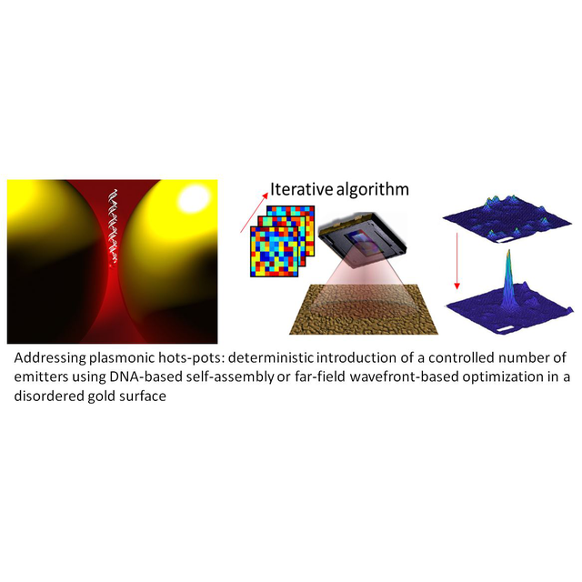
Addressing plasmonic hot-spots: from DNA-based self-assembly to far-field wavefront shaping
Centre de Nanosciences et de Nanotechnologies, Amphithéâtre, PalaiseauSeminars
Light-matter interactions in condensed media at room-temperature are fundamentally limited by electron-phonon coupling. For instance, while the excitation cross-section of an isolated atom, or of a single quantum emitter at cryogenic temperatures, can reach one half of the wavelength of light squared (meaning that ~50% of incoming photons will interact for a diffraction-limited excitation); this value is reduced by 6-7 orders of magnitude for a fluorescent molecule or for a colloidal quantum dot at room temperature because of homogeneous phonon broadening. In order to render the exceptional optical properties of single quantum systems (such as single-photon emission and nonlinearities) efficiently accessible at room temperature and in condensed media, it is essential to enhance and optimize these interaction cross-sections.
Over the last two decades, plasmonic resonators have shown amazing promise towards this goal thanks to their ability to enhance optical fields by several orders of magnitude in deeply sub-wavelength volumes. However, the nanoscale dimensions of these field enhancements or “hot-spots” mean that it is extremely difficult to exploit them in a controlled and reproducible way. At Institut Langevin, we develop two approaches in order to achieve this:
-We introduce, in a deterministic way, a controlled number of quantum emitters in the nanoscale hot-spot between two gold nanoparticles using a DNA-based self-assembly strategy. Using this approach, we were able to enhance single-photon emission from fluorescent molecules by more than two orders of magnitude in a weak-coupling regime. I will discuss recent experiments where we reach a strong-coupling regime between a plasmonic resonator and five organic molecules.
-We actively control the seemingly random plasmonic hot-spots featured by disordered gold surfaces using far-field wavefront shaping. In practice, by tuning the phase of a pulsed excitation, we ensure the constructive interference of plasmonic modes that are delocalized over several microns on the surface; leading to a local enhancement of the nonlinear luminescence of gold by more than two orders of magnitude.
Link: https://us02web.zoom.us/j/86277738532
Find a clickable link in the attached file below
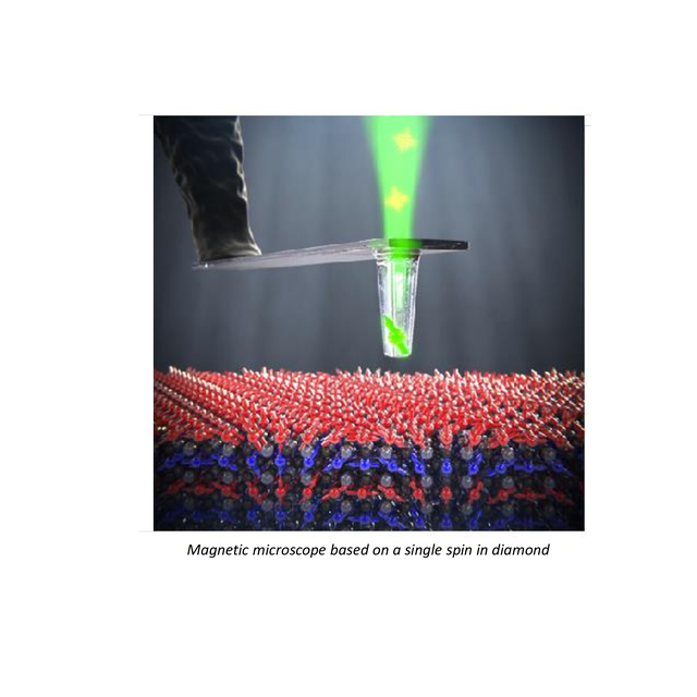
Exploring antiferromagnetic order at the nanoscale with a single spin microscope
Centre de Nanosciences et de Nanotechnologies, Amphithéâtre, PalaiseauSeminars
Experimental methods allowing for the detection of single spins in the solid-state, which were initially developed for quantum information science, open new avenues for the development of highly sensitive quantum sensors. In that context, the electronic spin of a single nitrogen-vacancy (NV) defect in diamond can be used as an atomic-sized magnetometer, providing an unprecedented combination of spatial resolution and magnetic sensitivity under ambient conditions. In this talk, I will illustrate how scanning-NV magnetometry can be used as a powerful tool for exploring condensed-matter physics, focusing on chiral spin textures in antiferromagnetic materials.
Dr. Vincent Jacques is a CNRS research associate in the team “Solid-state quantum technologies” at the Laboratoire Charles Coulomb (Montpellier). His research interests cover several fundamental and applied topics related to the applications of “artificial atoms” in quantum technologies. Such topics include quantum optics, spin physics, and quantum sensing with the development of highly-sensitive magnetometers based on NV defects.
Link: :https://us02web.zoom.us/j/86277738532
Find a clickable link in the attached file below

Integrated Lithium Niobate Photonics for Communication, Sensing and Quantum applications
Centre de Nanosciences et de Nanotechnologies, , PalaiseauSeminars
Lithium niobate (LN) is an “old” material with many applications in optical and microwave technologies, owing to its unique properties that include large second order nonlinear susceptibility, large piezoelectric response, and wide optical transparency window. Conventional discrete LN components, the workhorse of the optoelectronic industry for many decades, are reaching their limits, however. I will discuss our efforts aimed at the development of integrated LN photonic platform, featuring strong light confinement and dense integration, that has the potential to revolutionize optical communication networks and microwave photonic systems, as well as enable realization of quantum photonic circuits and integrated spectroscopic tools. Examples include high bandwidth, low voltage, and low loss electro-optic (EO) modulators [1], EO frequency combs [2], and programmable “photonic molecules” [3]. Devices that benefit from LN’s strong second and third order nonlinearity, including second harmonic generators [4] and Kerr frequency combs [5] will also be discussed.
1. C. Wang, M. Zhang, X. Chen, M. Bertrand, A. Shams-Ansari, S. Chandrasekhar, P. Winzer, and M. Lončar. “Integrated lithium niobate electro-optic modulators operating at CMOS-compatible voltages.” Nature, 562, 101 (2018)
2. M. Zhang, B. Buscaino, C. Wang, A. Shams-Ansari, C. Reimer, R. Zhu, J. Kahn, and M. Loncar. “Broadband electro-optic frequency comb generation in an integrated microring resonator.” Nature, 568, 373(2019)
3. M. Zhang, C. Wang, Y. Hu, A. Shams-Ansari, T. Ren, S. Fan, and M. Lončar. “Electronically Programmable Photonic Molecule.” Nature Photonics, 13, 36 (2019)
4. C. Wang, C. Langrock, A. Marandi, M. Jankowski, M. Zhang, B. Desiatov, M. M. Fejer, and M. Lončar. “Ultrahigh-efficiency wavelength conversion in nanophotonic periodically poled lithium niobate waveguides.” Optica, 5, 1438 (2018)
5. C. Wang, M. Zhang, M. Yu, R. Zhu, H. Hu, and M. Loncar, “Monolithic lithium niobate photonic circuits for Kerr frequency comb generation and modulation.” Nature Communications, 10, 978 (2019)
Marko Loncar is Tiantsai Lin Professor of Electrical Engineering at Harvard's John A Paulson School of Engineering and Applied Sciences (SEAS), as well as Harvard College Professor. Loncar received his Diploma from University of Belgrade (R. Serbia) in 1997, and his PhD from Caltech in 2003 (with Axel Scherer), both in Electrical Engineering. After completing his postdoctoral studies at Harvard (with Federico Capasso), he joined SEAS faculty in 2006. Loncar is expert in nanophotonics and nanofabrication, and his current research interests include quantum and nonlinear nanophotonics, quantum optomechanics, and nanofabrication. He has received NSF CAREER Award in 2009 and Sloan Fellowship in 2010. In recognition of his teaching activities, Loncar has been awarded Levenson Prize for Excellence in Undergraduate Teaching (2012), and has been named Harvard College Professor in 2017. Loncar is fellow of Optical Society of America, and Senior Member of IEEE and SPIE. He is co-founder of HyperLight Corporation, VC backed startup commercializing lithium-niobate technology developed in his lab.
Link: https://us02web.zoom.us/j/85124074169
Find a clickable link in the attached file below

Some key issues to model and characterize thermoelectric devices - Materials Department Seminar
Centre de Nanosciences et de Nanotechnologies, Amphithéatre, PalaiseauSeminars
Thermoelectricity has attracted the interest of the scientific community since its first observation by Thomas Seebeck in 1823. As a prototype of the most recent developments in finite-time thermodynamics, driven by the non-equilibrium thermodynamics formulated by Onsager (1931), thermoelectricity is of dual interest, both in fundamental and applied terms. In recent years, thermoelectricity has been the subject of major research efforts in the context of energy harvesting, aiming at direct conversion of heat into electricity using new non-toxic materials offering increased efficiency.
Beyond the interest of new materials for such a conversion, it is important to consider how to use these devices. First, the thermal contact between the device and the heat reservoirs is one of the key parameters that must be taken into account. In a first part, the impact of thermal contacts with the reservoirs will be described in order to extract the maximum power from the system. The key relationship between irreversibility and efficiency at maximum power can then be derived. The second issue concerns the ability to fully characterize thermoelectric materials and devices. To this end, recent advances in the use of nonlinear harmonic response will be illustrated for a standard thermoelectric system.
References:
[1] Y. Apertet, H. Ouerdane, O. Glavatskaya, C. Goupil, and Ph. Lecoeur "Optimal working conditions for thermoelectric generators with realistic thermal coupling". Europhysics Letters vol. 97, 28001 (2012).
[2] H. Ouerdane, Y. Apertet, C. Goupil, and Ph. Lecoeur "Continuity and boundary conditions in thermodynamics: From Carnot's efficiency to efficiencies at maximum power". European Physical Journal -- Special Topics vol. 224, 839 (2015).
[3] E. Thiébaut, F. Pesty, C. Goupil, G. Guegan, P. Lecoeur, Non-linear impedance spectroscopy for complete thermoelectric characterization: Beyond the zT estimation.Journal of Applied Physics 124 (23), 235106 (2018)
Link: https://teams.microsoft.com/l/meetup-join/19%3a8ef070af84874faeb64430eab7b45015%40thread.tacv2/1616088277667?context=%7b%22Tid%22%3a%2268cdfebb-157b-4846-ba2f-d196a9124ac0%22%2c%22Oid%22%3a%22583eb8c4-b43f-4ac4-a7d5-8939c7b2e5e8%22%7d
Find a clickable link in the attached file below
III-V and IV-IV heterogeneous integration on silicon at the nanoscale
Centre de Nanosciences et de Nanotechnologies, Amphithéâtre, PalaiseauSeminars
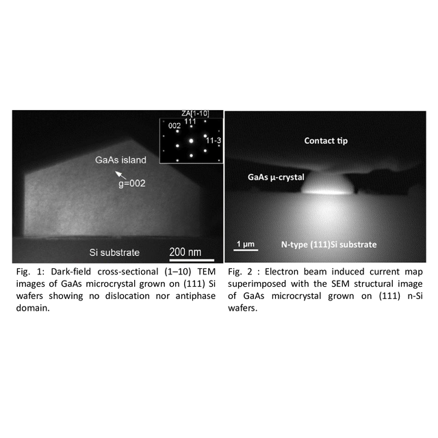
In this presentation, we will focus on the general problematic of heterogeneous integration on silicon of lattice mismatched materials, such as GaAs and germanium. After a brief introduction to this problem, I will present the concept of integration that we have developed to avoid the formation of crippling defects in this type of heterostructures (dislocations and antiphase domains). The concept adopted consists in carrying out growth from limited size seeds (<100nm) by partial deoxidation or localized etching of the substrate. I will then focus more particularly on the monolithic integration by lateral growth of GaAs micro-crystals from nanometric openings made through a thin layer of silica. We will then see that the electric current can cross the thin oxide zone separating the GaAs microcrystals and the silicon substrate, paving the way for the production of electrically injected optical components.
Charles Renard has performed his Ph.D. at Alcatel-Thales III-V Lab on the growth of Sb/As heterostructures for optoelectronic applications. Then he spent two years as a post-doctoral fellow at IEF on the growth of nanostructures for ultimate MOSFET. In 2008 he spent 6 months at IMEC, within the Ge III-V explore program. Since 2008, he is CNRS scientific researcher at IEF (now C2N) where he is working on hybrid integration of IV-IV materials on Si, since 2012 he expanded this study to III-V materials on Si. He obtained physics HDR degree in 2019.
Link: https://us02web.zoom.us/j/88274596539
Find a clickable link in the attached file below
Towards brain-inspired photonic computing - Departement of Photonics Seminar
Centre de Nanosciences et de Nanotechnologies, Amphithéâtre, PalaiseauSeminars
Photonic integrated circuits allow for designing computing architectures which process optical signals in analogy to electronic integrated circuits. Therein electrical connections are replaced with photonic waveguides which guide light to desired locations on chip. Through near-field coupling, such waveguides enable interactions with functional materials placed very close to the waveguide surface. This way, photonic circuits which are normally passive in their response are able to display active functionality and thus provide the means to build reconfigurable systems. By integrating phase-change materials nonvolatile components can be devised which allow for implementing hardware mimics of neural tissue. Here I will present our efforts on using such a platform for developing optical non-von Neumann computing devices. In these reconfigurable photonic circuits in-memory computing allows for overcoming separation between memory and central processing unit as a route towards artificial neural networks which operate entirely in the optical domain.
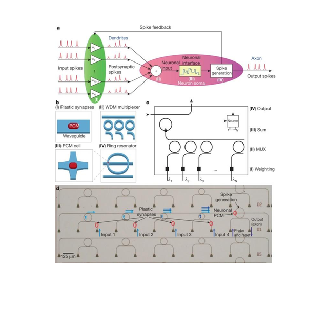
Figure: a, b, Schematic of the network realized in this study, consisting of several pre-synaptic input neurons and one post-synaptic output neuron connected via PCM synapses. The input spikes are weighted using PCM cells and summed up using a WDM multiplexer (MUX). If the integrated power of the post-synaptic spikes surpasses a certain threshold, the PCM cell on the ring resonator switches and an output pulse (neuronal spike) is generated. c, Photonic circuit diagram of an integrated optical neuron with symbol block shown in the inset (top right). Several of these blocks can be connected to larger networks using the wavelength inputs and outputs (see Fig. 5). d, Optical micrograph of three fabricated neurons (B5, D1 and D2), showing four input ports. The four small ring resonators on the left are used to couple light of different wavelengths from the inputs to a single waveguide, which then leads to the PCM cell at the crossing point with the large ring. The triangular structures on the bottom are grating couplers used to couple light onto and off the chip.
Link: https://us02web.zoom.us/j/87141030093
Find a clickable link in the attached file below

Ab-initio quantum transport simulation of layered 2D materials-based electron devices
Centre de Nanosciences et de Nanotechnologies, Amphithéâtre, PalaiseauSeminars
The prediction of electronic and transport properties of nanodevices based on recently synthetized materials such as layered two-dimensional materials demands the adoption of first-principles theories to avoid the use of empirical parameters. While the use of density functional theory (DFT) for band-structure calculations is fairly established, the adoption of a full ab-initio approach for electron transport investigations has been up to now limited due to its extremely high computational cost. This talk illustrates the theory and application of a first-principles transport methodology based on the non-equilibrium Green’s functions technique and employing a basis set obtained directly from the Bloch functions computed with a plane wave ab-initio solver. This enables full ab-initio quantum transport calculations with a good computational efficiency, and allows us to address self-consistent simulations of novel electronic devices. As an illustrative application, I will present an original device concept for energy-efficient, steep-slope transistors based on van der Waals heterojunctions of two-dimensional materials. In such a device, by injecting electrons from an isolated and weakly dispersive band into a strongly dispersive one, sub-thermionic subthreshold swings can be obtained, as a result of a cold-source effect and of a reduced thermalization of carriers.
Marco Pala received the physics degree and the PhD in electronical engineering from the University of Pisa, Italy in 2000 and 2004, respectively. From 2004 to 2005 he was post-doc at CEA-Leti, Grenoble, France. He entered at CNRS as research scientist in 2005 at IMEP-LAHC, Grenoble. From 2016 he is with the Centre for Nanoscience and Nanotechnology (C2N), Palaiseau, France, where is the leader of the computational electronics group. His main research interests concern the electronic and transport properties of nanoscale devices. Recently, he worked on quantum transport calculations based on ab-initio methods to assess the use of new materials in nanoelectronics.
Lien visio: https://us02web.zoom.us/j/89273446968
Topological Photonics - Departement of Photonics Seminar
Centre de Nanosciences et de Nanotechnologies, on line, PalaiseauSeminars
In the context of photonics, topology has emerged as an abstract, yet surprisingly powerful, new paradigm for controlling the flow of light. As such, it holds great promise for a wide range of advanced applications, from scatter-free routing and switching of light along arbitrary three-dimensional trajectories to long-distance transmission of slow-light waves. Whereas topological effects in condensed matter originate typically from the fermionic Kramer’s degeneracy or the quantum Hall effect in the presence of strong magnetic fields, these mechanisms cannot be readily adapted due to the bosonic nature of photons and the notoriously weak magnetic interactions at optical frequencies. Recently, a number of approaches for the realization of photonic topological transport have been put forward. Among these, perhaps the most promising one follows the spirit of Floquet topological insulators, in which temporal variations of solid-state systems induce topological edge states. In the context of photonics, temporal modulations serve to break the time-reversal symmetry and thereby give rise to topologically protected one-way edge states.
In my talk, I will present an introduction to topology in photonics, with a particular focus on our work on the implementation of photonic Floquet topological insulators. The purpose is to review these and other recent developments, to discuss potential applications and to stimulate new conceptual ideas.
Alexander Szameit was born in 1979 in Halle (Saale), Germany, and received his Physics Diploma, PhD, and his habilitation at the Friedrich-Schiller-Universität Jena (Germany) in 2004, 2007, and 2015, respectively. He was a visiting intern astronomer at the Institute for Astronomy in Hilo, HI in 2002 and a visiting fellow at the Nonlinear Physics Centre at the Australian National University in 2007. He spent from 2009-2011 as PostDoc at the Technion in Haifa (Israel) and returned in 2011 as Assistant Professor to Jena. Since 2016, he is full professor for experimental solid-state optics at the University of Rostock.
Alex Szameit’s research includes various aspects of modern optics, such as linear and nonlinear waves in periodic media, micro and nano-photonics, the integration of complex optical circuits and chip-based photonic quantum computing. He published more than 200 peer-reviewed papers in internationally recognized scientific journals, including Nature, Nature Photonics, Nature Materials, Nature Physics, Nature Communications and Physical Review Letters, and gave more than 150 invited presentations and colloquiae. His current h-index is 54 with more than 9000 citations in total.
Link: https://us02web.zoom.us/j/85302866256