
Soutenance HdR
(en anglais) Controlling Magnetism by Interface Engineering
Centre de Nanosciences et de Nanotechnologies, Salles A005-A007-A009, PalaiseauSoutenance HdR
Jury members:
Prof. Stéphane Mangin, Université de Lorraine, Nancy, rapporteur
Dr. Jean-Philippe Attané, CEA Grenoble, Grenoble, rapporteur
Prof. Massimiliano Marangolo, Institut des NanoSciences de Paris, Paris, rapporteur
Dr. Stefania Pizzini, Institut Néel, Grenoble, examinateur
Prof. Vincent Jeudy, Laboratoire de Physique de Solides, Palaiseau, examinateur
Dr. Mohamed Belmeguenai, Laboratoire des Sciences des Procédés et des Matériaux, Villetaneuse, examinateur
Dr. Dafiné Ravelosona, Centre de Nanosciences et Nanotechnologies, Palaiseau, examinateur
Abstract :
In this thesis I describe diverse strategies to control magnetism in nanostructured systems by acting on the structural and electronic properties of interfaces.I will present how light ion irradiation induces atomic intermixing at the top and bottom interfaces of thin magnetic materials with perpendicular anisotropy and its effect on the magnetic properties and disorder. An important part will be dedicated to the effects of electric fields on the magnetic properties of metallic thin films in solid state and liquid gate devices exploiting different physical mechanisms such as charge accumulation and ionic displacement. I will also show examples of the useof surface functionalisation to introduce new degrees of freedom, such as light sensitivity, for the control of magnetic properties in ferromagnetic semiconductors. These examples will show a glimpse of the variety of physical effects that can be triggered at interfaces and the potential of interface engineering to unveil new physical effects and to contribute to the development of novel practical applications in spintronics.
Lisa Herrera Diez has an interdisciplinary background in physics and chemistry. She studied physical chemistry at the National University of Cordoba (Argentina) and conducted her doctoral studies at the Max-Planck Institute for Solid State Research while enrolled in the physics doctoral school at Ecole Polytechnique Federale de Lausanne (2008-2010). During this time she performed studies on magnetic domain wall dynamics and magneto-transport in devices based on diluted ferromagnetic semiconductors. From 2011 to 2012 she worked as a postdoctoral researcher at Institut Neel in Grenoble. During this postdoctoral stay she worked on electric
field control of magnetic anisotropy and domain wall dynamics in metallic ferromagnetic devices. Since 2013 she is a CNRS researcher at C2N and her main scientific
interests are oriented towards the control of domain wall dynamics in multifunctional nanodevices.
Intégration de semiconducteurs III-V et IV-IV sur silicium à l’échelle nanométrique
Ecole Polytechnique, Amphithéâtre Cauchy, Palaiseau CedexSoutenance HdR
Jury members :
Chantal FONTAINE, Rapporteur 1
Thierry BARON, Rapporteur 2
Charles CORNET, Rapporteur 3
Bruno GERARD, Examinateur 1
Gilles PATRIARCHE, Examinateur 2
Daniel BOUCHIER, Examinateur 3
Abstract :
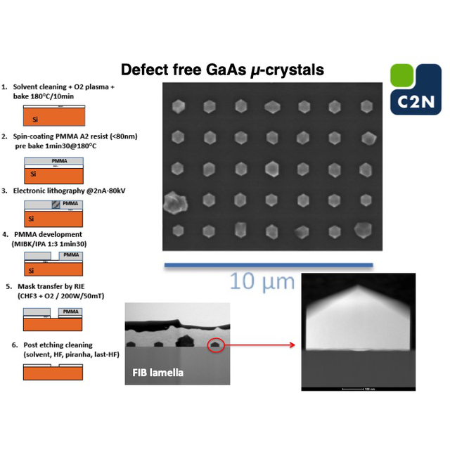
Mes activités de recherche au C2N portent sur la problématique générale de l'intégration hétérogène sur silicium de matériaux désaccordés, tels que le GaAs et le germanium. Après une brève introduction de cette problématique, je présenterai le concept d’intégration que nous avons développé pour éviter la formation de défauts rédhibitoires dans ce type d’hétérostructures (dislocations liées à la relaxation et défauts d'antiphase dans les couches III-V/IV). Le concept adopté consiste à réaliser la croissance à partir de germes limités en taille (<100nm) par désoxydation partielle, gravure localisée du substrat ou en faisant croître des nanofils.
Je m’intéresserai ensuite plus particulièrement à l’intégration monolithique par croissance latérale de micro-cristaux de GaAs à partir d’ouvertures nanométriques réalisées au travers d’une fine couche de silice. Nous verrons alors que le courant électrique peut traverser la zone d’oxyde mince séparant les micro-cristaux de GaAs et le substrat de silicium, ouvrant la voie à la réalisation de composants optiques injectés électriquement.