
Séminaires
(en anglais) Quantum thermal transport in circuits
Centre de Nanosciences et de Nanotechnologies, Amphithéâtre, PalaiseauSéminaires
Heating drives a crossover from quantum to classical behaviors. However, heat itself is ruled by the laws of quantum mechanics. In small electrical circuits, the fundamental implications span from a different quantum thermodynamics to the quantum phase influence on heat. In addition, the flow of heat provides a revealing and complementary probe for the investigation of intriguing phases of matter, by unveiling neutral states invisible to electrical transport. In the long term, quantum thermal phenomena will ineluctably constitute an essential parameter for the quantum engineering of nanocircuits. Other envisioned possibilities include novel calorimetry devices and thermal machines.
Whereas the quantum transport of electricity is being actively investigated since more than three decades, the thermal facet is more challenging to access. In particular, there is no equivalent of the ammeter for the flow of heat. Only recently experimental observations are emerging, such as the universal thermal conductance quantum, heat interferometry, or the heat conductance across a superconducting quantum bit. After a general introduction of the field, I will present the experimental determination of the universal limit imposed to heat flow by quantum mechanics, and the observation of heat Coulomb blockade, a many-body quantum effect that can selectively apply to heat but not to electricity in violation of the standard Wiedemann-Franz law.
External visitors should be register beforehand (follow the link in the attached file)
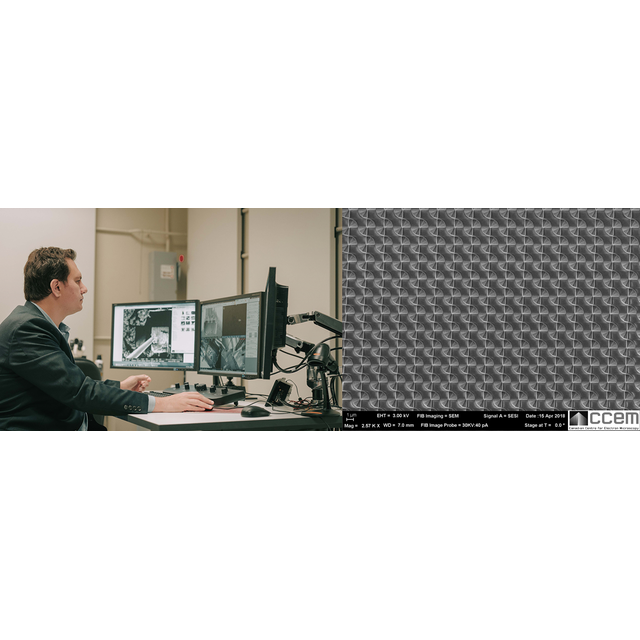
(en anglais) New Developments in the Application of Focused Ion Beam Technology – Sources + Computation + Ions = Better FIB SCIence.
Centre de Nanosciences et de Nanotechnologies, Amphithéatre, PalaiseauSéminaires
Focused Ion Beam (FIB) technology has much of its roots in the semiconductor industry, for circuit edit, mask repair and, later for TEM lamella sample preparation. Powered by its long-standing front-running ion source technology, the gallium-based liquid metal ion source, FIB has been developed for a number of applications beyond sample preparation, including serial sectioning, in situ techniques, and direct-write patterning. Furthermore, in recent years, the two major developments have opened new avenues of research in FIB technology: the first is the rapid development of new source technologies, including plasma sources, liquid metal alloy sources, and gas field ion sources, which brings much of the periodic table to bear for novel applications. The second is the advent of computational microscopy, in which scanning systems are evolving to allow high-speed characterization and on-the-fly adjustment during FIB and electron source use.
In this talk, I will show how these two new developments have expanded the boundaries of our thinking about FIB technology through several examples. The first is in the development of new electronic and optical materials based on ion implantation using novel sources and direct-write lithography. Following, this, I will demonstrate serial sectioning methods using plasma FIB for large-volume mesoscale applications. We will show that data processing and the use of on-the-fly sparse scanning with offline reconstructions can make dealing with large datasets more feasible and faster.
Nabil BASSIM
Associate Professor, Department of Materials Science and Engineering, McMaster University, Hamilton, Ontario,08/2016–present
Materials Research Engineer, Materials Science and Technology Division, U.S. Naval Research Laboratory, Washington, DC, USA
2008–2016
Postdoc: National Institute of Standards and Technology,2006-2007
Postdoc: Electronic Division: U.S. Naval Research Laboratory,2003-2006
Ph.D.: University of Florida,2002
(en anglais) Coupling organic molecules to nanophotonic structures
Centre de Nanosciences et de Nanotechnologies, Salle A003, PalaiseauSéminaires
Photons lie at the heart of many quantum technologies. They are the only logical choice for sending quantum information over long distances, they have been used for many demonstrations of quantum simulations, they are often employed in microscopy to perform high‐resolution imaging and they are promising candidates for quantum computing and networking. Still, they are difficult to generate and collect with high efficiency. In this talk I will discuss the use of organic molecules for generating, processing and storing single photons. When dibenzoterrylene (DBT) is embedded in anthracene it is photostable and forms a two‐level system which when excited will emit a photon at a wavelength of ~780 nm. This is desirable as a number of atomic quantum technologies based on rubidium interact efficiently with light at this wavelength. When cooled to 4K, DBT can be used to generate coherent, lifetime‐limited photons. I will show our work in characterising a single molecule at temperatures down to 4 K and show that coherent Rabi oscillations are then seen in the excited state population. I will then discuss our recent work to couple the emission from single molecules into nanophotonic waveguides including hybrid plasmonic systems and dielectric nanowire waveguides crossed with organic filled micro‐capillaries. Finally I will discuss the use of nanophotonic and optical fibre cavities to further enhance the collection of photons from single molecules.
External visitors should be register (follow the link in the attached file)
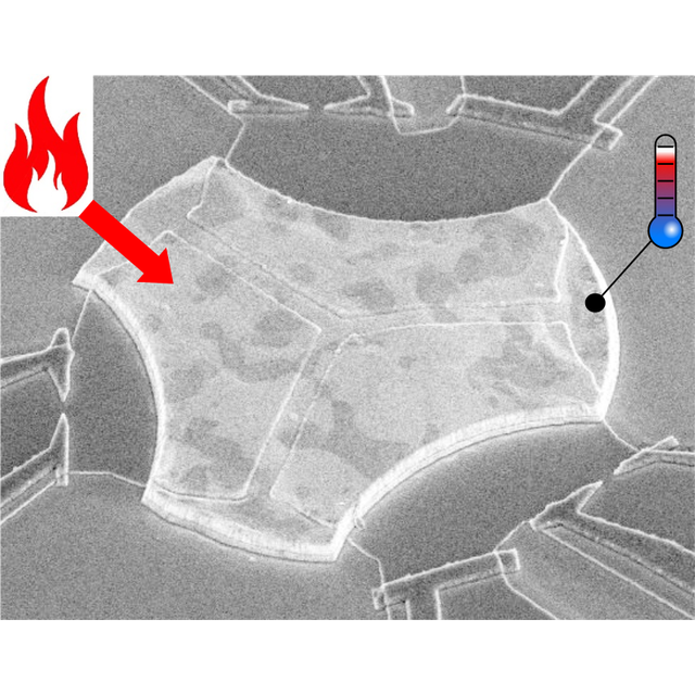
(en anglais) Quantum effects at superconducting phase transitions
Centre de Nanosciences et de Nanotechnologies, Amphithéatre, PalaiseauSéminaires
While superconductivity is the archetype of quantum matter, with an entangled ground state of time-reversed states, the superconducting order parameter is essentially a classical field as a consequence of the Bose condensation of a macroscopic number of Cooper pairs. Yet, in some situations, the quantum dynamic of this superconducting order parameter can be observed experimentally. In a first example, I will show that the transport properties of superconducting thin films near the superconductor-insulator transition follow scaling laws that reflect the increased quantum fluctuations across the phase transition. In a second example, I will describe a Scanning Tunneling Spectroscopy (STS) study of the superconducting properties of ultra high vacuum (UHV) grown Pb nanocrystals where we identified a lower size limit for the existence of superconductivity. This size limit, called the Anderson limit, is the consequence of quantum fluctuations in pairing amplitude and is reached when the electronic level spacing becomes larger than the superconducting pairing energy. Finally, I will describe the project of Electron-Spin-Resonant- STM spectroscopy developed in the STM group of C2N, an experimental method that has potential applications for the study of quantum dynamics in atomically precise spin systems.
Legend: UHV grown superconducting Pb nanocrystals on InAs
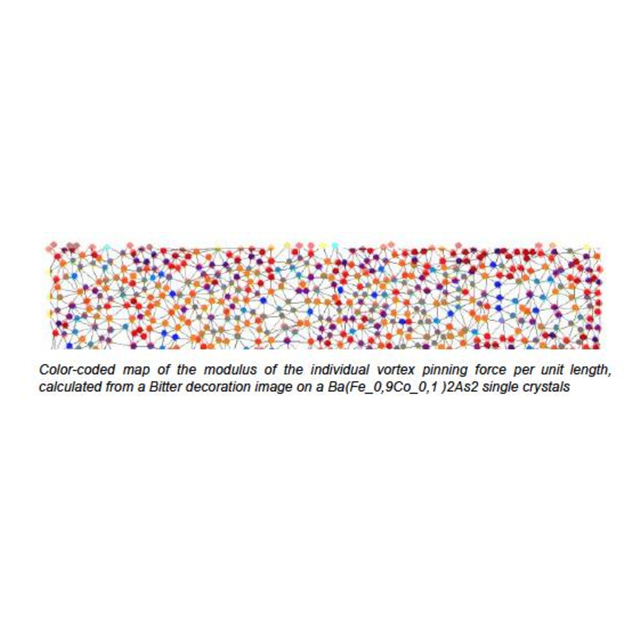
(en anglais) Some current trends in the physics of superconducting flux vortices
Centre de Nanosciences et de Nanotechnologies, Amphithéâtre, PalaiseauSéminaires
Owing to the prospect of spectacular dissipation-less applications such as powerful magnets and exquisitely sensitive detectors with an ever-smaller need for refrigeration of the material, the discovery of new classes of high temperature superconducting materials is usually
accompanied by much excitement. However, fashioning actual superconducting applications meets with different limitations of fundamental, material, and technological nature. At the same time, type II superconductors, in which the magnetic field partially permeates the material in the form of quantized flux lines (or vortices), provide an exciting playground for the study of different flux-line aggregation states.
In this presentation, I shall briefly dwell on the state of the art in the field of superconductivity, before describing some examples of recent research on vortex physics: the interaction of vortex lines with disorder and the occurrence of different vortex states in the iron-based high temperature superconductors, and the physics and application of cuprate high temperature superconducting films for RF and HF current limiting devices. I shall finish with a number of perspectives.
External visitors should be register
(en anglais) “Spin-Orbit Technologies: From Magnetic Memory to Terahertz Generation”
Centre de Nanosciences et de Nanotechnologies, Amphithéatre, PalaiseauSéminaires
Abstract:
Spintronic devices utilize an electric current to alter the state of a magnetic material and thus find great applications in magnetic memory. Over the last decade, spintronic research has focused largely on techniques based on spin-orbit coupling, such as spin-orbit torques (SOTs), to alter the magnetic state. The phenomenon of spin-orbit coupling in magnetic heterostructures was also recently used to generate terahertz emission and thus bridge the gap between spintronics and optoelectronics research.
I will introduce the basic concepts of SOTs, such as their physical origin, the effect of SOTs on a magnetic material, and how to quantitatively measure this effect [1,2]. Next, I will discuss the latest trends in SOT research, such as the exploration of novel material systems like topological insulators and two-dimensional materials to improve the operation efficiency [2,3]. Following this, some of the technical challenges in SOT-based magnetic memory will be highlighted [3]. Moving forward, I will introduce the process of terahertz generation in magnetic heterostructures [4], where the spin-orbit coupling phenomenon plays a dominant role. I will discuss the details of how this terahertz emission process can be extended to novel material systems such as ferrimagnets [5] and topological materials [6]. The final section will focus on how the terahertz generation process can be used to measure SOTs in magnetic heterostructures, thus highlighting the interrelation between terahertz generation and the SOTs, which are linked by the underlying spin-orbit coupling.
[1] X. Qiu et al., “Characterization and manipulation of spin orbit torque in magnetic heterostructures,” Adv. Mater., 30, 1705699 (2018).
[2] Y. Wang et al., “FMR-related phenomena in spintronic devices” J. Phys. D: Appl. Phys., 51, 273002 (2018).
[3] R. Ramaswamy et al., “Recent advances in spin-orbit torques: Moving towards device applications” Appl. Phys. Rev., 5, 031107 (2018).
[4] Y. Wu et al., “High-performance THz emitters based on ferromagnetic/nonmagnetic heterostructures” Adv. Mater., 29, 1603031 (2017).
[5] M. Chen, et al., “Terahertz emission from compensated magnetic heterostructures,” Adv. Opt. Mater., 6, 1800430 (2018).
[6] X. Wang, et al., “Ultrafast spin-to-charge conversion at the surface of topological insulator thin films” Adv. Mater. 30, 1802356 (2018).
Hyunsoo Yang obtained the bachelor’s degree from Seoul National University and the PhD degree from Stanford University. He worked at C&S Technology, Seoul; LG Electronics, San Jose, CA; and Intelligent Fiber Optic Systems, Sunnyvale, CA, USA. From 2004 to 2007, he was at the IBM-Stanford Spintronic Science and Applications Center, IBM Almaden Research Center. He is currently a GlobalFoundries chaired associate professor in the Department of Electrical and Computer Engineering, National University of Singapore, working on various magnetic materials and devices for spintronics applications. He has authored 170 journal articles, given 100 invited presentations, and holds 15 patents. Prof. Yang was a recipient of the Outstanding Dissertation Award for 2006 from the American Physical Society’s Topical Group on Magnetism and Its Applications and the IEEE Magnetic Society Distinguished Lecturer for 2019.
*** IMPORTANT ***
Participants external to the C2N laboratory must register using the form below in order to attend the seminar:
https://framaforms.org/registration-c2n-seminar-dr-hyunsoo-yang-spin-orbit-technologies-from-magnetic-memory-to-terahertz-0
(en anglais) Twistable electronics with dynamically rotatable heterostructures
Centre de Nanosciences et de Nanotechnologies, Amphithéatre, PalaiseauSéminaires
A simple, yet effective, way to modify the properties of 2D materials is by stacking them in a
van der Waals heterostructures and controlling the relative angular orientation between its
layers. This in situ band structure manipulation offers unique opportunities toward
understanding of multiple physical phenomena and the design of novel opto-electronic
devices. A striking example of this is the recent observation of strongly correlated states and
intrinsic superconductivity in twisted bilayer graphene. The clearest example of the effects of
angular alignment in a heterostructure is graphene on hexagonal boron nitride (BN), in which
the layer orientation determines the wavelength of a superimposed moiré superlattice. The superpotential modifies the native band structure of graphene opening an energy gap and generating minigaps at higher energies. However, current techniques are limited to
fabrication of samples with fixed interlayer angles. Studies of angular dependence are therefore limited to static properties, and require multiple samples, which imposes experimental challenges and introduces uncertainty due to sample-to-sample variations.
In this talk I will present a new technique which allows to modify in situ optical, mechanical and electronic properties of a BN/graphene/BN heterostructures, in this the angle between layers is changed continuously with a control better than 0.2 degrees. Combining these three
measurements in the same device demonstrates the new capability to precisely tune in situ the properties of a van der Waals heterostructure. Our new experimental technique opens the possibility to study the angle-dependent properties of van der Waals heterostructures and in situ band structure engineering of 2D materials.
(en anglais) A multiscale approach to interfacial magnetism
C2N, Amphithéatre, PalaiseauSéminaires
Interface phenomena are becoming crucial for devices such as in magnetic random-access memories (MRAM) [1]. Interfaces can host a wide range of phenomena: the changes of chemical potential can induce large electric fields and the breaking of inversion symmetry allows the emergence of new transport properties or new interactions. The study of material properties at this scale requires to understand the interplay between chemical, structural and functional properties at the microscopic scale. This can be achieved based on atomistic simulations parametrized via density functional theory (DFT) calculations. Recently, magnetism interfaces have been attracting lots of attention due to the presence of a chiral interfacial interaction called the Dzyaloshinskii-Moriya interaction (DMI). The DMI stabilizes chiral non-collinear magnetic textures such as domain-walls or skyrmions which can be manipulated efficiently by electrical currents and offer attractive perspectives for future spintronic applications [2].
I will describe how density functional theory can be used to accurately describe the stability of non-collinear magnetic textures at surfaces [3] and interfaces [4]. In particular, I will show that atomistic Hamiltonians parametrized via DFT calculations can be used to engineer the magnetic properties of interfaces and explain the occurrence of skyrmions and their transport properties [5]. Our microscopic models reveal that a new type of magneto-resistance, called the non-collinear magnetoresistance (NCMR), can emerge depending on the skyrmion radius [10]. Our methods further allow the exploration of the stabilization mechanisms of skyrmions. We also show that the competition between magnetic interactions can give rise to the simultaneous stabilization of both skyrmion and anti-skyrmions with peculiar dynamical properties [6]. Our findings suggest new mechanisms to nucleate skyrmions such as magnetization quenching [7] or ultra-fast laser pulses [8]. These achievements show that Hamiltonians parametrized via DFT are a powerful tool to design materials with tuned magnetic, ferroelectric, and optical properties.
[1] B. Dieny et al., Reviews of Modern Physics 89, 025008 (2017).
[2] A. Fert et al., Nature Nanotechnology 8, 152 (2013).
[3] M. Hervé, B. Dupé et al., Nature Communications 9, 1015, (2018).
[4] B. Dupé, et al., Nature Communications 7, 11779 (2016).
[5] C. Hanneken, B. Dupé et al., Nature Nanotechnology 10, 1039 (2015).
[6] U. Ritzmann, B. Dupé et al. Nature Electronics 1, 451 (2018).
[7] I. Lemesh, B. Dupé et al., Advanced Materials 30, 1805461 (2018).
[8] B. Pfau, B. Dupé et al., in preparation.
*** IMPORTANT ***
Participants external to the C2N laboratory must register using the form below in order to attend the seminar:
https://framaforms.org/registration-c2n-seminar-dr-bertrand-dupe-1551881586
(en anglais) Building artificial quantum materials with light
C2N, Amphithéâtre, PalaiseauSéminaires
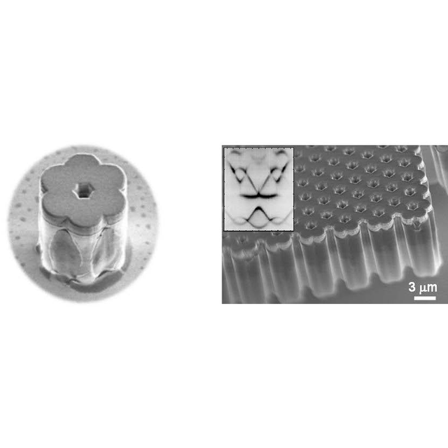
Engineering strong interactions between optical photons is a great challenge for quantum science and technology. One envisioned application is the realization of synthetic quantum materials as a tool to harness and investigate quantum-correlated systems.
Polaritonics, based on the strong coupling of photons to atomic or electronic excitations in an optical resonator, have proved to be a particularly versatile platform to engineer diverse photonic materials. However, it has also been shown that going into the quantum regime requires polariton-polariton interactions that are an order of magnitude stronger than what is currently achieved in state-of-the-art samples.
I will present two approaches that are being developed to tackle this challenge. I will first describe experiments performed at ETH Zürich demonstrating that polariton-polariton interactions can be significantly enhanced by embedding a high-mobility 2D electron system in an optical cavity: an order of magnitude enhancement over the interactions is obtained when the electrons of the 2DES are initially in a fractional quantum Hall state. I will then discuss perspectives related to the development of new active materials exhibiting excitons with a permanent dipole, an approach which is potentially compatible with polariton lattices developed at C2N.
External visitors should be register beforehand. Follow the link on the attached file.
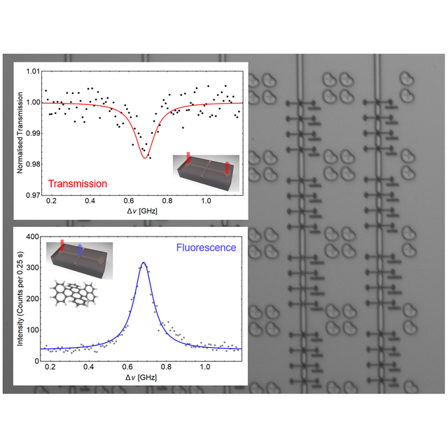
Figure : SEM images photonic materials built at C2N
(en anglais) Real time TEM observation of semiconductor nanowire growth
C2N site Palaiseau, Amphithéatre, PalaiseauSéminaires
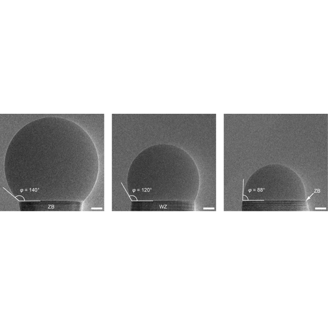
Synthetizing III-V semiconductor nanowires (NWs) using the vapour-liquid-solid (VLS) method can result in the growth of crystal structures different from their bulk phase. In GaAs NWs, for example, the stable phase zinc-blende (ZB) coexists with the metastable wurtzite (WZ) structure. Remarkably, the valence and conduction bands are misaligned in the two phases, so that small sections of one phase within the other effectively confine charge carriers along the wire axis. Therefore, the possibility of controllably switching between phases opens up opportunities to create novel heterostructures commonly identified as crystal phase quantum dots (CPQD). In contrast to compositional heterojunctions, crystal phase heterostructures have the intrinsic property of minimizing residual strain and alloy intermixing at interfaces.
In this talk, I will present experimental observations of the growth of Ga-As nanowires obtained using a transmission electron microscope (ETEM) equipped with molecular-beam-epitaxy (MBE) sources. NWs are grown directly inside the microscope and their growth is monitored in situ and in real time with high spatial and temporal resolution. I will show that thanks to these new insights we can precisely dictate the crystal phase and diameter of nanowires in order to synthetize CPQD with unprecedented control on their size and position along the wire axis. I will then discuss the opportunities that this novel family of structures opens up for the fabrication of single photon emitters and other photonic devices.
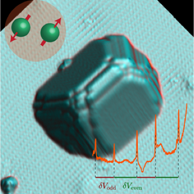
TEM images showing the impact of the droplet aspect ratio on the crystal structure of self-catalyzed GaAs NWs.