News released (in French) by the Institut des Sciences et de l’Ingénierie des Systèmes (INSIS) of CNRS on 25 November 2019
Despite their excellent energy performance, some solar panels are still too expensive to be used widely. Researchers from the Laboratoire Nanotechnologies et Nanosystèmes (LN2), the Centre de Nanosciences et de Nanotechnologies (C2N) and the University of Warwick (UK) have managed to reduce the costs of multi-junction solar cells thanks to the use of nanoporous germanium. This work, that enables to reduce the presence of defects on different crystalline substrates, was published in Nature Communications.
Multi-junction solar cells offer excellent performance, but at a cost that is still too high. The incident light must be concentrated by lenses to make the system more profitable, which is not enough yet to compete with conventional solar cells. Researchers from the Laboratoire nanotechnologies et nanosystèmes - LN2 (international joint research unit* between France and Canada), the Centre de nanosciences et de nanotechnologies** - C2N (CNRS/Université Paris-Saclay) and the University of Warwick in the United-Kingdom managed to lower the price thanks to the use of nanoporous germanium.
Solar cells need a crystalline substrate, representing about a third of the total cost. It usually means a 150 micron layer of germanium for multi-junction cells, which could be replaced by silicon that is much cheaper. However, the contact between silicon, germanium and the cell causes the appearance of defects and leads to a decrease of the energy yields. To solve this problem, the researchers inserted a layer of only 2 microns of nanoporous germanium between the silicon and the rest of the cell. Some defects still appear, but they are totally erased with a process of electrochemical etching. Costs are halved, while the performance is improved. This technique can also be used to integrate III-V semiconductors, such as gallium arsenide, which are interesting for many applications in electronics. The team is now looking for new opportunities and collaborations.
- Read the news (in French) on the website of the Université de Sherbrooke.
* Between CNRS, Université de Sherbrooke, Université de Lyon – Ecole Centrale de Lyon, INSA and CPE/Université Grenoble Alpes
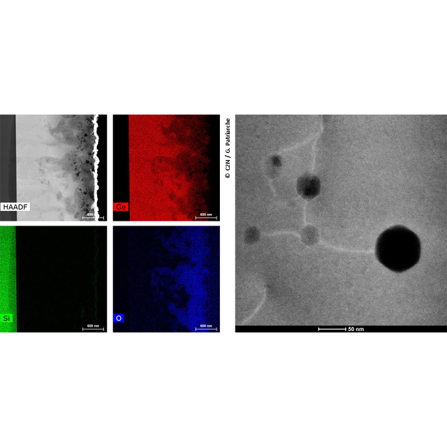
** Most of the structural characterization studies were performed with the Transmission Electron Microscope (TEM) Titan Themis at C2N (Material Analysis Platform – Materials Department). See Figure.
Reference:
Uprooting defects to enable high-performance III–V optoelectronic devices on silicon
Youcef A. Bioud, Abderraouf Boucherif, Maksym Myronov, Ali Soltani, Gilles Patriarche, Nadi Braidy, Mourad Jellite, Dominique Drouin & Richard Arès
Nature Communications - volume 10, article number: 4322 (2019)
https://www.nature.com/articles/s41467-019-12353-9
Contacts:
Richard Ares, LN2
Gilles Patriarche, CNRS Senior Researcher at C2N
Figure: (left) Elemental chemical mapping by STEM-EDX of a nano-porous germanium layer. (right) Threading dislocations present in the epitaxial layer of germanium anchored by the nanopores - STEM image in dark field (HAADF). © C2N / G. Patriarche