![]() Service Communication
Service Communication
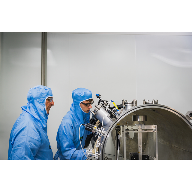
Année de l'ingénierie: a video at the heart of C2N's research on the photonic quantum computer
As part of the Année de l'ingénierie, CNRS is partnering with Bloom Média to make engineering, its scientific research and its professions accessible, tangible and …