• 410

    people

  • 120

    Researchers

  • 80

    engineers, technicians and admnistrative staff

  • 18 000 sqm

    incl. 2 800 sqm of cleanroom facility

  • 4

    Research departments

  • 2

    International Research Projects (IRP CNRS)

  • 1

    technology facility

  • 3

    platforms of expertise

C2N

A CNRS - Université Paris-Saclay and Université Paris Cité joint research unit

The Centre for Nanosciences and Nanotechnology (C2N) is a joint research unit between the CNRS and Université Paris-Saclay. It was founded on the 1stJune 2016 by merging two former laboratories, the Laboratoire de Photonique et de Nanostructures (LPN) and the Institut d’Electronique Fondamentale (IEF). In 2018, the laboratory moved to a new building at the heart of Campus Paris-Saclay, in the south of Paris.


The Board of Directors of the Centre for Nanosciences and Nanotechnology  consists of the laboratory Director, Giancarlo Faini, four deputy directors : Laurent Vivien, Arnaud Bournel, Pierre-Yves Joubert and Jean-Christophe Harmand, as well as a General-secretary, Cynthia Vallerand.


Le C2N

The creation of C2N on the Plateau de Saclay was done within  an ambitious perspective. The laboratory benefits from its very favorable location for exchanges with academic laboratories and with the R&D of the local industrial cluster. It brings together the former teams of the IEF and the LPN and gathers critical forces on key lines of research. It meets two principal and inseparable objectives:

  • To establish a flagship laboratory for research in nanoscience and nanotechnology
  • To provide a large technology facility to the Plateau de Saclay and the Ile-de-France region, open to all academic and industrial players in the field, especially those from the Paris region


Science at C2N

The center develops research in the field of material science, nanophotonics, nanoelectronics, nanobiotechnologies and microsystems, as well as in nanotechnologies. In all these fields, its research activites cover all the range from fondamental to applied science. The laboratory is organized around 4 scientific departments:

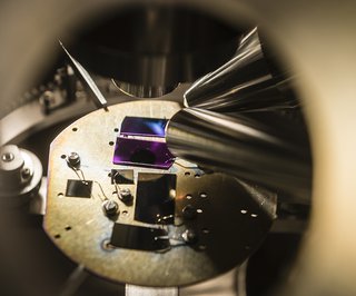
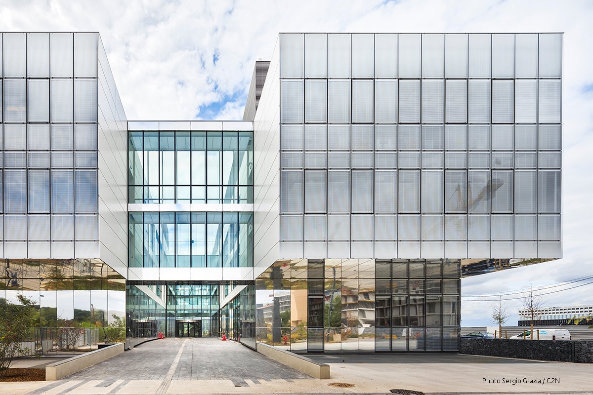
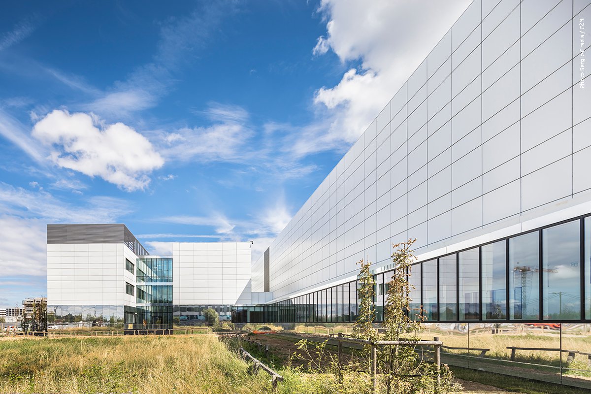
Photonics department

Read more

Research activities in photonics focuse simultaneously on fundamental reasearch (such as control and manipulation of quantum information) as well as on applied research for short- or mid-term applications in the field of information technologies, photovoltaics or biomedical imaging and sensors. Gathering more than 180 members, this department is one of the major European pole of expertise in photonics.

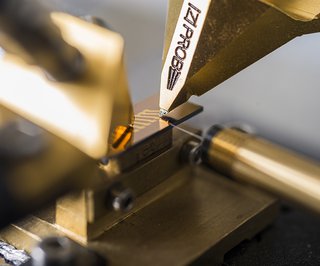
Three inter-related axes are developed: Nonlinear and quantum nanophotonics, Subwavelength photonics and nano-objects and Photonics and nanophotonics devices.

Materials Department

Read more

Material science is at the core of a large majority of research topics at C2N. Innovating in this field is of crucial importance.Understanding growth mechanisms and correlating the material properties with their growing conditions, is one of the main challenge of the department. These objectives make use of advanced synthesis, growth and analysis techniques as well as the development of adpated theoretical and numerical tools. Activities in material science focuse mainly on nanostructures made of III-V semiconductors, Si/Ge, novel 2D materials, functional oxides and metals. Hybridization of various materials is another challenge, opening the way to the implementation of novel functionalities. These activities are pursued in strong interaction with photonics, nanoelectronics, devices and systems.

6 inter-realted axes are developed: Small-dimensionality objects, Hybridization, Mixed interfaces, Topological materials, Integration stratégies, Theory, modeling and simulation, and Analysis..

Nanoelectronics Department

Read more

Exploiting new physical concepts occuring at nanoscale, research activities in nanoelectronics cover a broad spectrum ranging from the fundamental investigation of quantum circuits to the implementation of novel nanodevices based on the manipulation of various variables (charge, spin, phase), including the development of novel architectures such as bioinspired circuits. Two inter-related axes are developed: Nanoscale physics in novel charge and spindevices and Innovative architectures.

The department of nanoelectronics is strongly involved in partnerships with other players on the Saclay Plateau as well as with major industrial companies to open up new applications area. All these players, gathered on the plateau, constitue one of the main European pole of expertise in spin electronics and nanophysics.

Microsystems and Nanobiofluidics Department

Read more

Nanoelectromechanical systems (NEMS), whose emergence is recent, have shown a very high potential for the investigation of fundamental physical phenomena or for the implementation of ultra-sensitive sensors and miniaturized clocks.

Moreover, applications of micro-nano-technologies in the health field, constitute a major research domain, in particular in the Île-de-France region that gathers a large number of university-affiliated hospitals.

3 inter-related axes are developed: Micro- Nano- Systems and Instrumentation, Micro- Nano- Devices for biomedical applications and Micro- Nano- Fluidics and biotechnologies.

Advanced instrumentation
 

Its strong instrumentation activity makes C2N a world-class player in the development of new instruments for nanotechnology. With these instruments, nano-objects are realized, analyzed and measured with ultimate control and spatio-temporal resolutions. These instruments are also developed and commercialized in partnership with leading equipment manufacturers.