
HdR defense
(in french)
C2N - Centre de Nanosciences et de Nanotechnologies, , PalaiseauHdR defense
Along the edges of crystal growth:planar, nanostructured and van der Waals epitaxy
C2N - Centre de Nanosciences et de Nanotechnologies, , PalaiseauHdR defense
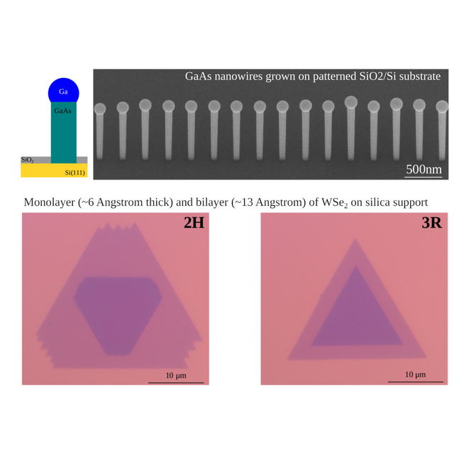
Many semiconducting materials used in electronic devices are crystalline solids, in which atoms are ordered by well-defined symmetries. These synthetic (man-made) crystalline solids are obtained routinely in research laboratories or industry by standard crystal growth techniques, such as molecular beam epitaxy (MBE) or chemical vapor deposition (CVD).
Most devices combine several functions, such as light emitter (quantum wells), electrical contacts (doping) or light confinement (cladding layers). As a result, a single material is usually not enough and the crystal properties must be varied along the structure to alter the electronic band gap, the carrier concentration or the optical index. As one crystal seamlessly merges into another, the electronic bands are engineered into complex heterostructures in a deterministic manner.
For a given crystalline semiconductor, there are physical constraints which restrict the defect-free growth of one crystal onto another. In practice, the unit cell parameters, symmetry, thermal mismatch or chemical nature impose severe limitations, which separate semiconductors into distinct and incompatible families.
Here, we rationalize the impact of these fundamental limitations in practical case studies such as “How to maintain the planar character of smooth planar layers during growth? ”, “Why grow on expensive monocrystalline substrates while cheap amorphous supports are available?”, “What are advantages and the drawbacks of nanostructuration?” and “Why does van der Waals epitaxy look attractive compared to conventional epitaxy and where is the catch?”.
(in french)
C2N - Centre de Nanosciences et de Nanotechnologies, , PalaiseauHdR defense