

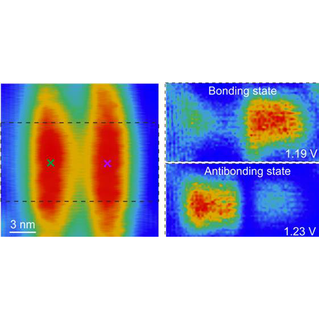
Thanks to an advanced technique of scanning tunnelling microscopy and spectroscopy (STM/STS), a team of researchers at C2N was able to observe the electronic coupling of a pair of quantum dots using simultaneous imaging of morphology and electronic density of state.
In the context of quantum technologies, the control of the coupling between confined nanostructures such as cavities, resonators, or quantum dots is essential. This coupling is key to increase the interaction between electrons, phonons or photons, and thus to observe new properties useful for the development of nano-devices. The nature and strength of the interaction are often measured indirectly and on an assembly of dissimilar objects. An important issue today is to be able to measure the interaction between individual and finely characterized nano-objects.
A team of researchers at C2N adopted an innovative point of view by using a specific technique, cross-sectional scanning tunneling microscopy and spectroscopy (STM/STS). They were able to directly map the electronic coupling of individual pairs of self-assembled quantum dots. This work was published in Nano Letters.
The STM/STS equipment allowed, after cliving under ultra-vacuum, to simultaneously image the morphology and the density of electronic coupling of pairs of In(Ga)As/GaAs self-assembled Quantum Dots (QDs) forming Quantum Dots Molecules (QDMs). The researchers highlighted the formation of binding and anti-binding electronic states for these "artificial molecules". Thanks to the support of numerical simulations, they showed the importance of taking into account the exact geometry of the pairs of boxes (i.e. shape, size and distance between boxes), for determining the strength of the coupling.
Reference:
Real Space Observation of Electronic Coupling between Self- Assembled Quantum Dots
G. Rodary, L. Bernardi, C. David, B. Fain, A. Lemaître & J.-C. Girard
Nano Letters (2019), 19, 3699−3706
DOI : https://doi.org/10.1021/acs.nanolett.9b00772
Contacts:
Guillemin Rodary, CNRS researcher at C2N
Jean-Christophe Girard, CNRS researcher at C2N
Figure: Left: STM topographic image of a pair of In(Ga)As/GaAs self-assembled Quantum Dots. Right: image of differential conductance (i.e. local electronic state density) of the binding and anti-binding states of the artificial molecule formed from the pair of quantum dots. Crédits: C2N

