Positive and negative electric charges attract each other, forming atoms, molecules, and all that we usually refer as matter. Negative charges instead repel each other, and in order to form atom-like bound objects some extra glue is needed, in order to compensate this electrostatic repulsion and bind the particles together.
In a paper recently published in the journal Nature Physics, researchers at C2N, in an international collaboration with University of Southampton (UK), University Trento and Laboratorio TASC (Italy), demonstrated that photons, the particles which compose light, can be used to glue together negative charges, creating a novel form of matter they named a Photon Bound Exciton.
The result implements experimentally a theoretical prediction published last year by the same team. First, a nano-device that traps electrons into nanoscopic wells was implemented. It was shown that photons of high enough energy striking the device extract electrons from the wells, similarly to the photoelectric effect. Subsequently, the system has been enclosed between two gold mirrors, which trap the photons and dramatically increase the interaction between light and matter. The team observed that a negatively-charged electron kicked out by a photon then remains instead trapped in the well, bound to the other negatively-charged electrons in an electronic configuration now stabilized by the photon. In the collaboration, C2N was in charge of the experimental work.
The result demonstrates the possibility of engineering novel artificial atoms with designed electronic configurations, expanding the list of materials available for scientific and technological applications.
Reference:
Excitons bound by photon exchange
Erika Cortese1, Linh Tran2, Jean-Michel Manceau2, Adel Bousseksou2, Iacopo Carusotto3, Giorgio Biasiol4, Raffaele Colombelli2 and Simone De Liberato1
Nature Physics (2020)
DOI : https://doi.org/10.1038/s41567-020-0994-6
1 School of Physics and Astronomy, University of Southampton
2 Centre de Nanosciences et de Nanotechnologies - C2N (CNRS/Université Paris-Saclay), Palaiseau, France
3 INO-CNR BEC Center and Dipartimento di Fisica, Universita di Trento
4 Laboratorio TASC, CNR-IOM, Trieste
Contact:
- Raffaele Colombelli, CNRS Senior Researcher at C2N
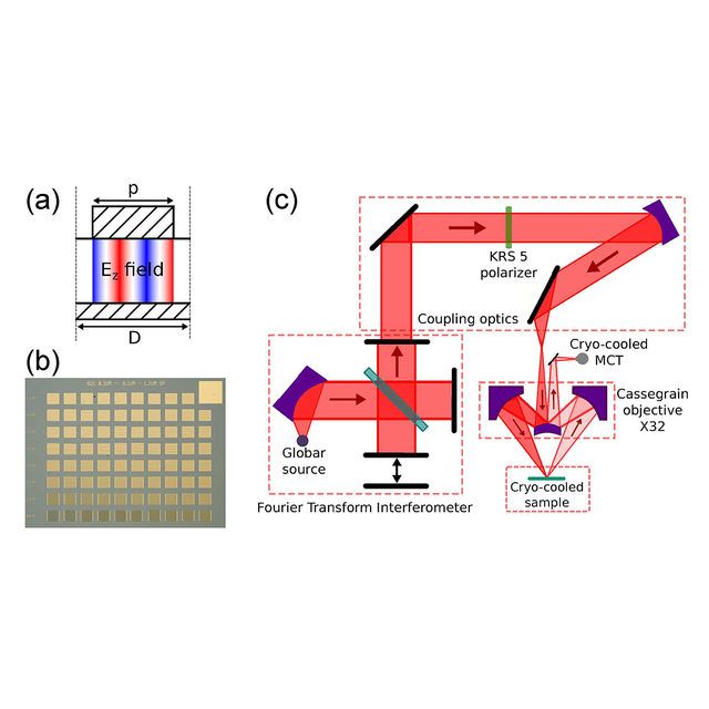
Figure: a) Distribution of the electric field component orthogonal to the metallic layers for one period of the structure.
The resonators are one-dimensional ribbons (or 1D patch cavities) that enclose the semiconductor active region. The picture shows that the electromagnetic field is almost completely confined below the metallic fingers.
b) Optical microscope image of a typical sample set. Each device features a different finger width p.
c) The experimental set-up used for the reflectivity measurements. It consists of a mid-infrared microscope connected to an FTIR spectrometer. The source is a thermal globar lamp, and the detector is a liquid-nitrogen-cooled mercury–cadmium telluride (MCT). A compact, thin cryostat permits measurements to be performed down to a temperature of 78 K.