

Abstract
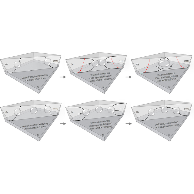
High-quality germanium epilayers on Si with low threading-dislocation density were achieved by sintering of porous Ge/Si films. The process consists in the formation of porous Ge nanostructures by dislocation-selective electrochemical etching of Ge/Si films, followed by high-temperature treatment to generate a monocrystalline, voided Ge layer that intercepts dislocations and prevents them from propagating to the sample surface. In this work, we model the morphological changes that occur during the thermal treatment-induced surface diffusion of an axially symmetric hole. Simulations and experiments show individual large spherical voids, aligned along the dislocation core. The creation of voids could facilitate interactions between dislocations, enabling the dislocation network to change its connectivity in a way that facilitates the subsequent annihilation of dislocation segments. This confirms that thermally activated processes such as state diffusion of porous materials provide mechanisms whereby the defects are removed or arranged in configurations of lower energy. This demonstration paves the way to develop a virtual substrate on many other heterostructures for potential applications in integrated photonic and optoelectronic devices.

