The optical and electrical characteristics of electrically-driven nanogap antennas are extremely sensitive to the nanogap region where the fields are tightly confined and electrons and photons can interplay. Upon injecting electrons in the nanogap, a conductance channel opens between the metal surfaces modifying the plasmon charge distribution and therefore inducing an electrical tuning of the gap plasmon resonance. Electron tunneling across the nanogap can be harnessed to induce broadband photon emission with boosted quantum efficiency. Under certain conditions, the energy of the emitted photons exceeds the energy of electrons, and this overbias light emission is due to spontaneous emission of the hot electron distribution in the electrode. We conclude with the potential of electrically controlled nanogap antennas for faster on-chip communication.
The concentration of light at scales well below the wavelength has been made possible thanks to the structuring of metallic objects which support collective oscillations of electrons (plasmonics) when they interact with electromagnetic radiation. This localization effect produces field enhancements of several orders of magnitude relative to the incident value. The efficiency of light-matter interactions is then greatly increased and confined to the nanometric scale, which has had an impact on a wide variety of applications.
The design, at selected wavelengths, of plasmon resonances and the corresponding strong fields has been the subject of many studies. Their realization was strongly supported by modern techniques of nano-fabrication and nano-characterization, which allowed the detailed study of the optical properties of metallic nanostructures, isolated or grouped into dimers, trimers, oligomers or supracrystalline films.
Dimer structures were found to be particularly effective at confining light, allowing stronger mode volume reduction than with single nanoparticles. The nanometric gap between the two monomers (nanogap), by allowing the control of the localized plasmon coupling and the confinement volume, has opened up new horizons for various applications.
This result motivated researchers to explore the properties of space-separated metallic nanostructures at the nanoscale. It has been shown that quantum effects strongly affect the plasmonic and electric fields of interacting nanostructures. Indeed, when the width of the gap is small enough, electrons can pass from one nanoparticle to another by tunnel effect. When a voltage is applied between these nanoparticles, these electrons can relax their excess energy by emitting a photon. This gives them interesting electroluminescence properties for the design of electrically driven devices for the emission or detection of light at the nanometric scale and with ultrafast operation.
This article reviews recent work on these nanostructures, also called “nanogap antennas”. It provides a clear overview of the fundamental optoelectronic properties, as well as the possibilities and constraints of fabricating these nanostructures.
Références
Electrically driven nanogap antennas and quantum tunneling regime
1Claire Deeb, 2Johann Toudert and 3Jean-Luc Pelouard
Nanophotonics 12(15) : 3029–3051 (2023)
DOI: https://doi.org/10.1515/nanoph-2023-0099
Affiliations
1 Almae Technologies, Route de Nozay, 91460 Marcoussis, France
2 Ensemble3 Centre of Excellence, Warsaw, Polan
3 Centre for Nanoscience and Nanotechnology - C2N, CNRS, Université Paris-Saclay, 10 Bvd T. Gobert, 91120 Palaiseau, France
Keywords
hot carriers; inelastic electron tunneling; nanogap antennas; photon emission; quantum regime; tunnel junction
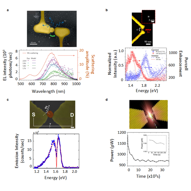
Figure : Examples of in-plane nanogap antennas showing inelastic electron tunneling-induced electroluminescence: tuning the emission spectrum, pattern and optimizing the radiated power