

On-chip spatial and polarization multiplexing has emerged as a powerful strategy to boost the data transmission capacity of integrated optical transceivers. State-of-the-art multiplexers require accurate control of the relative phase or the spatial distribution among different guided optical modes, seriously compromising the optical transmission bandwidth and performance of the devices. To overcome this limitation C2N researchers, in collaboration with the QuTech and Kavli Institute of Nanoscience and the Telecommunication Research Institute (TELMA), have demonstrated a new approach based on the coupling between guided modes in integrated waveguides and optical beams free-propagating on the chip plane. The engineering of the evanescent coupling between the guided modes and free-propagating beams allows spatial and polarization multiplexing with state-of-the-art performance. A two-polarization multiplexed link and a three-mode multiplexed link using standard 220-nm-thick silicon-on-insulator technology have been developed. The two-polarization link shows a measured −35 dB crosstalk bandwidth of 180 nm, while the three-mode link exhibits a −20 dB crosstalk bandwidth of 195 nm. These links are used to demonstrate error-free operation (bit-error-rate <10−9) in multiplexing and demultiplexing of two and three non-return-to-zero signals at 40 Gbps each, with power penalties below 0.08 and 1.5 dB for the two-polarization and three-mode links, respectively. The approach demonstrated for two polarizations and three modes is transferable to future implementation of more complex multiplexing schemes. These findings, recently published in the journal Laser & Photonics Review, pave the way for the next generation of high-speed and large-capacity on-chip optical interconnects, quantum information sciences, optical sensing, on-chip wireless communications, and nonlinear photonics.
Silicon photonics has been identified as a promising technology to address the traffic bottleneck in data centers and networks facing communication growing. Current silicon photonics optical transceivers carry different data channels at distinct wavelengths using wavelength-division multiplexing. However, as the industry moves forward with the development of next-generation optical networks, other multiplexing schemes will be required to support a higher data capacity per wavelength channel. One promising approach is the use of spatially-distributed modes to encode more data channels at a specific wavelength combining even orthogonal polarization modes as in current systems with low-loss multiplexer.
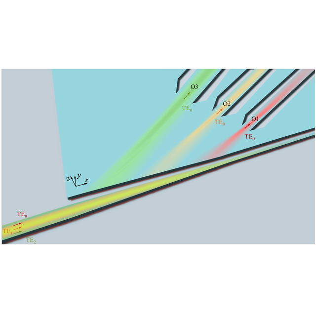
A myriad of architectures has been proposed to realize mode-division and polarization-division multiplexing. Despite the great diversity of proposed solutions, crosstalk still remains as one of the main impairments in high-speed optical communications, especially in systems with a high-channel count. An increased crosstalk has a negative impact on the link performance in terms of bit-error-rate (BER) and ultimately results in a power penalty that jeopardizes low power consumption. In this work, a fundamentally new approach to realize highly efficient mode and polarization (de)multiplexing is proposed. Specifically, the evanescent coupling between the modes of a photonic waveguide and free-propagating beams on the chip plane is engineered to make each waveguide mode (or polarization) couple to a different in-plane beam, propagating with a specific angle. The proposed three-mode link comprising a multiplexer and a demultiplexer shows a measured crosstalk lower than −20 dB over a 195 nm bandwidth (1443–1638 nm) that fully covers the S, C, and L telecommunication bands, and partially covers the E and U bands. On the other hand, the two-polarization link yields an ultra-low crosstalk below −35 dB within the 1500–1680 nm wavelength range for both polarizations (covering the entire C, L, and U bands, and part of the S band). A high-speed optical communications demonstration was also performed to illustrate the applicability of the proposed devices. Transmission of two and three non-return-to-zero signals at 40 Gbps each was demonstrated, with power penalties below 0.08 and 1.5 dB for the two-polarization and three-mode links, respectively, at a BER of 10−9 without using any correction technique.
The low crosstalk, wide bandwidth, and versatility of the proposed multiplexing approach presented in this work open up unique possibilities in quantum information sciences, optical sensing, on-chip wireless communications, and nonlinear photonics.
Références
González-Andrade, D.1, Le Roux, X.1, Aubin, G.1, Amar, F.1, Nguyen, T. H. N.1, Nuño Ruano, P.1, Dinh, T. T. D., Oser, D.1,2, Pérez-Galacho, D.3, Cassan, E.1, Marris-Morini, D.1, Vivien, L.1, Alonso-Ramos, C.1,
Spatial and Polarization Division Multiplexing Harnessing On-Chip Optical Beam Forming.
Laser Photonics Rev 2023, 2300298.
DOI : https://doi.org/10.1002/lpor.202300298
Affiliations
1 Centre de Nanosciences et de Nanotechnologies, CNRS, Université Paris-Saclay, Palaiseau 91120, France
2 Institut des nanosciences QuTech et Kavli, Université de Technologie de Delft, Delft 2600 GA, Pays-Bas
3 Institut de Recherche sur les Télécommunications (TELMA), CEI Andalucía TECH, Université de Malaga, Malaga 29010, Espagne
Contacts
David Gonzalez Andrade
Carlos Ramos
Keywords : Integrated optics, Optical beam forming, Polarization division multiplexing, Silicon photonics, Slab, Spatial division multiplexing
Figure : Three-dimensional view of one of the proposed devices, showing the handling of three modes enabled by on-chip optical beamforming in an integrated circuit. The simulated electric field distribution in the xy-plane is superimposed on the structure when TE0 (red), TE1 (orange), and TE2 (green) modes are injected in the waveguide. Output waveguide apertures are located at the focal points to collect the free-propagating beams.

