

A C2N team, in collaboration with the LNE and the Geeps has developed a multiple resistance wide range calibration sample compatible with any commercially available AFM system.
Measuring resistances at the nanoscale has attracted recent attention for developing microelectronic components, memory devices, molecular electronics, and two-dimensional materials. Despite the decisive contribution of scanning probe microscopy in imaging resistance and current variations, measurements have remained restricted to qualitative comparisons. Reference resistance calibration samples are key to advancing the research-to-manufacturing process of nanoscale devices and materials through calibrated, reliable, and comparable measurements. No such calibration reference samples have been proposed so far.
In this work, we demonstrate the development of a multi-resistance reference sample for calibrating resistance measurements in conductive probe atomic force microscopy (C-AFM) covering the range from 100 Ω to 100 GΩ. We present a comprehensive protocol for in situ calibration of the whole measurement circuit encompassing the tip, the current sensing device, and the system controller. Furthermore, we show that our developed resistance reference enables the calibration of C-AFM with a combined relative uncertainty (given at one standard deviation) lower than 2.5% over an extended range from 10 kΩ to 100 GΩ and lower than 1% for a reduced range from 1 MΩ to 50 GΩ. Our findings break through the long-standing bottleneck in C-AFM measurements, providing a universal means for adopting calibrated resistance measurements at the nanoscale in the industrial and academic research and development sectors.
We are continuing the development of these calibration samples and are currently working on another version that offers easier access to C-AFM measurements of lower resistances (from 100 Ω to 10 kΩ) and an expanded resistance range up to 1 TΩ. This research work was carried out in the framework of the ELENA project (EMPIR 20IND12), which is supported by the European Metrology Programme for Innovation and Research (EMPIR).
References
Multi-Resistance Wide-Range Calibration sample for Conductive probe Atomic Force Microscopy Measurements
François Piquemal1, Khaled Kaja1, Pascal Chrétien2,3, José Morán‐Meza1, Frédéric Houzé2,3, Christian Ulysse4 and Abdelmounaim Harouri4
Beilstein J. Nanotechnol. 2023, 14, 1141–1148
DOI: https://doi.org/10.3762/bjnano.14.94
Affiliations
1Laboratoire national de métrologie et d’essais - LNE, Trappes, 78197 Cedex, France
2Université Paris-Saclay, CentraleSupélec, CNRS, Laboratoire de Génie Électrique et Électronique de Paris, 91192, Gif-sur-Yvette, France
3Sorbonne Université, CNRS, Laboratoire de Génie Électrique et Électronique de Paris, 75250, Paris, France
4Centre de Nanosciences et de Nanotechnologies - C2N, Université Paris-Saclay, CNRS, UMR 9001, Palaiseau, 91120, France
Contacts : christian.ulysse@c2n.upsaclay.fr, francois.piquemal@lne.fr
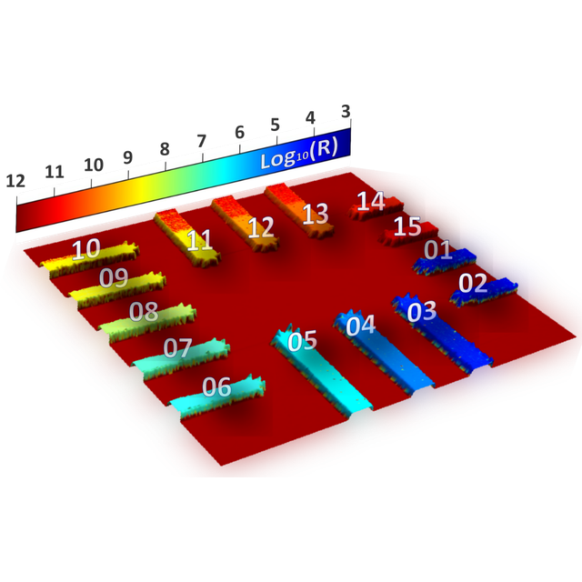
Figure : Resistance map of the sample’s central zone (60 µm × 60 µm) imaged by C-AFM. Numbers refer to the i index of the resistance arms. Colors rendering refers to measured resistance values given in decimal logarithm scale.
Mots-Clefs
Resistance standard; Conductive probe Atomic Force Microscopy; Calibration; nanoscale; Measurement protocol

