Ajouter à son agenda
 Gaia Maffione
Soutenance de thèse
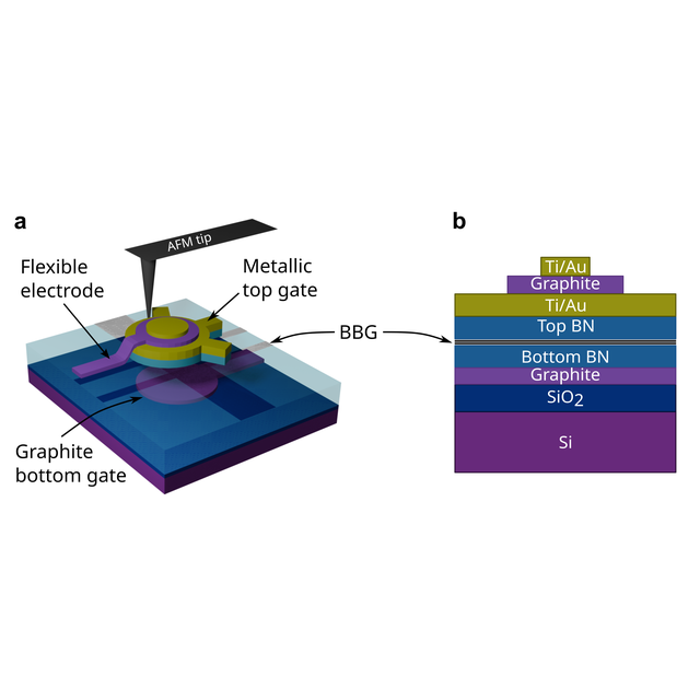
Two-dimensional materials can be stacked into van der Waals heterostructures, exhibiting novel properties tunable through layer combination, interlayer spacing and crystallographic alignment. This thesis experimentally investigates the effects of moiré superlattice and perpendicular electric field on the electronic properties of heterostructures based on Bernal bilayer graphene (BBG) and hexagonal boron nitride (BN). Using dynamically rotatable devices, we tune the relative angle between graphene and the top BN layer via AFM tip driven rotation. Dual gated rotatable devices, developed during the thesis, allow to independently tune carrier density and displacement field while retaining angular control.
Charge transport measurements in local and non-local configurations, from low to high temperatures, reveal distinct electronic properties at 0° and 60° alignments of BBG and BN. Numerical simulations attribute these differences to distinct in-plane atomic relaxation at the two alignments, arising from inequivalent stacking configurations. Using dual gated devices, we disentangle the respective impact of moiré superlattice and displacement field in opening an energy gap at the charge neutrality point of BBG, revealing a non-trivial angular dependence of the built-in crystal field, in agreement with simulations. We further observe the anomalous gating effect in BN/BBG/BN heterostructures, marked by gate-induced hysteresis and gate ineffectiveness, and we identify the 30° ± 15° rotation between the two BN layers as the triggering parameter. We show that this effect can be switched ON and OFF by rotating the top BN layer, with angle control shifting the device between three distinct metastable states.
Together, these results show that the twist angle affects the properties of van der Waals heterostructures not only through the alignment of the main active layers, but through the angular configuration of all layers involved.
Jury members :
Figure 1. (a) and (b), Schematics of a dual gated rotatable device and its cross section. The device is composed of: Si/SiO2 substrate, graphite bottom gate, bottom BN flake, BBG Hall bar, top gate made of BN/Ti/Au rotator and flexible graphite electrode.
Amphithéâtre
Centre de nanosciences et de nanotechnologies
10 bld Thomas Gobert
91120 Palaiseau