Ajouter à son agenda
 Owen Loison
Soutenance de thèse
In this thesis, we are interested in the Esaki diode, invented by Leo Esaki in 1957. This device exploits electronic tunneling and allows for good performance in sources and detectors. The Esaki diode is also the building block of the tunnel field-effect transistor which is a promising candidate for low-power electronics. However, the Esaki diodes made of conventional materials suffer from several drawbacks like sensitivity to defects at the heterostructure interface. 2D materials, and especially Transition Metal Dichalcogenides (TMD), are expected to yield better performance in tunnel diodes thanks to their ability to form heterostructures with good interface properties and a wide variety of band alignments. In this work, we investigate, through numerical simulations, the performance of Esaki diode made of TMD van der Waals heterostructures. First, we study the electronic properties of four TMDs: WSe2, HfSe2, SnSe2 and TaSe2 with the use of Density Functional Theory (DFT). We build heterostructures with these materials and determine which combination yields the best band structure in the objective of building a tunnel device. We also study the effects of the number of layers. Then, we study the vibrational properties of these TMDs. Phonons can influence the structure of the materials and the electron-phonon coupling will affect the electronic transport. We explain and use a method to compute this electron-phonon coupling from first principles. The transport calculations are done with the NEGF formalism. In order to lighten the computational load and allow for the study of large heterostructures, we introduce a multi-band Hamiltonian model. Since tunneling is at the heart of Esaki diodes, the tunneling coupling between the bands is the most important physical parameter. Therefore, instead of a constant parameter, we choose to use a coupling which depends on the electric field. The model for the coupling is then verified against DFT. The other parameters of the Hamiltonian are also calibrated with the ab initio calculations conducted just beforehand. Finally, the electron-phonon coupling is added thanks to the previous calculations. The transport calculations are then conducted on devices made using the monolayer/monolayer and trilayer/trilayer SnSe2/WSe2 heterostructures. We can probe the influence of different parameters of the simulation like the overlap length. With the trilayer/trilayer heterostructure, we can approach the experimental conditions. To go further, we propose simple expressions to add real phenomena that are not described by our model: valley current and contact resistance. With these additions and the model we developed, we are able to qualitatively reproduce the current-voltage characteristic of an Esaki diode made of TMDs.
Jury members:
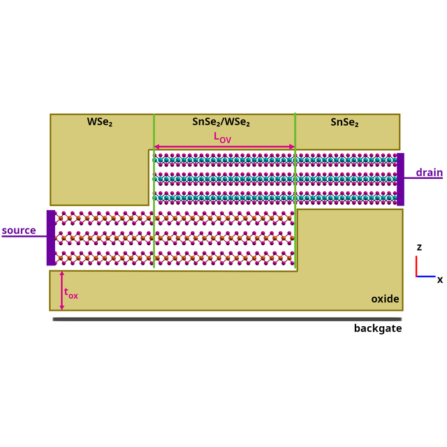
Figure : Illustration of an Esaki diode based on the trilayer/trilayer SnSe2/WSe2 heterostructure (not to scale). The tunneling occurs in the region where WSe2 and SnSe2 overlap. A back gate with a tunable voltage sits at the bottom of the device.
Amphithéâtre
10 boulevard Thomas Gobert
10 boulevard Thomas Gobert
91120 Palaiseau