
Séminaires
(en anglais) Optical Nanofibers; experiments in optomechanics and quantum optics.
C2N site Marcoussis, Salle R. Planel, NozaySéminaires
Nanofibers produced by tapering an ordinary single mode optical fiber to diameters of half a micron are interesting optical objects. We have studied the Spin-optomechanical coupling between light and a nanofiber torsional mode with nanofibers excited with circularly polarized light in the HE11 mode. Our recent experiments with cold trapped Rb atoms around the nanofiber include the modification of the polarization of the light by the birefringence of the atoms,revealing their dynamics in the trap.
Work supported by the National Science Foundation of the United Stated.

(en anglais) Heat Assisted Magnetic Recording Technology - Background, Status and Future
C2N site Orsay, salle 44, Orsay CedexSéminaires
Heat-assisted magnetic recording (HAMR) media requirements and challenges to extend the areal density (AD) beyond 1.4 Tb/in2 [1] will be discussed. Industry research efforts started in 2000 and Hard Disk Drives (HDD) with capacities beyond 10 Terra-Bytes (TB) per disk drive are expected in 2018 [2]. Key progress efforts beyond recording media are related to read-write heads, head-disk interface (HDI) and channels. Today’s channels allow experimental bit-error rates (BER) down to 10-2 [1].
Todays HAMR media are based on granular high magnetic anisotropy chemically ordered, well textured and chemically isolated L10 FePtX-Y films of about 12 nm average thickness. This is achievable by sputter co-deposition of FePt with grain segregants, Y, like C, BN, SiO2 or TiO2 (carbides, nitrides, oxides). Such segregants laterally exchange-decouple grains and make them permanent magnets with up- or down orientation. Six to ten of such grains form one bit with either up (=1) or down (=0) orientation.
Key ongoing progress efforts include average grain diameter <D> reduction from 8 to 4 nm, grain diameter distribution reduction sD/D from 20 to 10 % and Curie temperature distributions sTC/TC below 3%. Research and development efforts are adjusting / optimizing TC to the available near field transducer (NFT) laser heat power by doping FePt with Cu or Ni. Thin seed layers like 10 nm thick fcc MgO (100) are important to facilitate the formation of well-oriented grains with high chemical ordering and proper perpendicular magnetic anisotropy Ku > 5.107 erg/cm3 [3]. All this is expected to increase AD up to about 4 Tb/in2 [3]. Other, primarily modeling efforts, predict at least 10 Tb/in2 AD HAMR technology, e.g. based on exchange coupled continuous ECC media, which will also be highlighted.
[1] Ganping Ju et al., IEEE Trans Mag. 51, 3201709 (2015)
[2] Mark Re, Seagate (2016)
[3] D. Weller et al., pss A, 210, 1245, (2013) & D. Weller et al., IEEE Trans Mag 50, 3100108 (2014)
(en anglais) NITRIDE CHEMICAL PASSIVATION OF AIIIBV SEMICONDUCTOR SURFACES: CHEMISTRY, POSSIBLE APPLICATIONS
C2N site Orsay, salle 44, Orsay CedexSéminaires
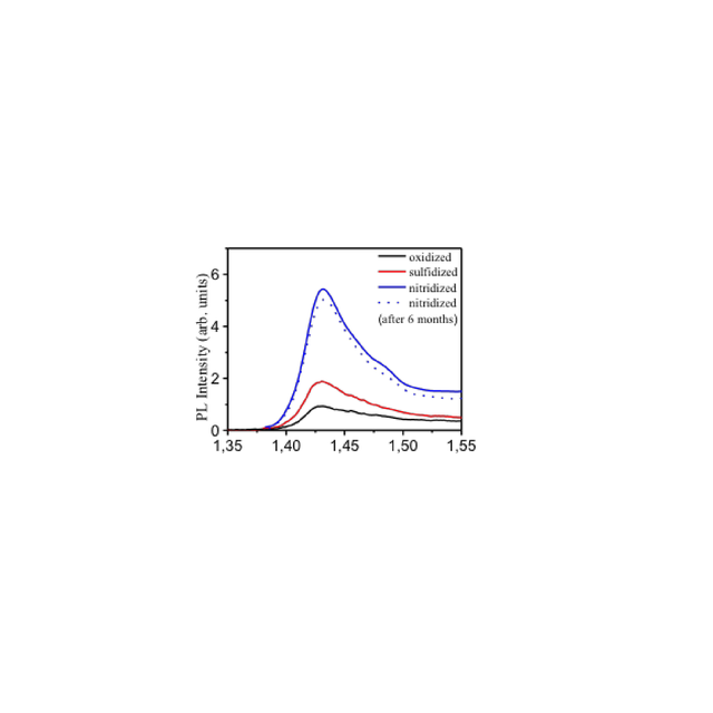
A wet chemical nitridation procedure in hydrazine–sulfide solutions has been developed for surface passivation of A3B5 semiconductors. For GaAs and GaSb this procedure allows to create a monolayer of GaN coherently bonded with surface atoms of these crystals. Due to high stability of Ga-N bond, the formed nitride minolayer protects the semiconductor surfaces against oxidation in atmospheric ambient. In also provides an effective electronic passivation.
Chemical processes occurring in GaAs surface in the hydrazine-sulfide solution are explained.
Some experimental results evidencing to chemical and electronic passivation of the nitidized GaAs surfaces are presented. Finally, a number of possible applications of the wet nitridation including passivation of GaAs nanowires are demonstrated.
Légend:
Surface chemical nitridation of GaAs nanowires (NW) reduces the surface state density by a factor of 6 that gives rise to essential increase of the NW conductivity and microphotoluminescence intensity
(en anglais) Auto-generators of sinusoidal and pulsed THz-frequency signals based on antiferromagnetic dielectrics driven by spin current
C2N site Orsay, salle 44, Orsay CedexSéminaires
Antiferromagnets (AFM) are seen as materials for novel THz-frequency signal processing devices [1,2]. In contrast to the devices based on ferromagnets (FM), the AFM-based devices do not require any external bias magnetic field. Also, the ultrafast magnetization dynamics of the AFM devices is determined by the strong internal exchange field that exists in AFM materials, and keeps their magnetic sublattices anti-parallel to each other. This exchange field determines the high natural frequencies of the AFM resonance, lying in the sub-THz to THz frequency range. Thus, it is tempting to use AFM as active layers in THz-frequency spin-torque nano-oscillators, where the output electromagnetic signal is received using the inverse spin-Hall effect (ISHE) in the NiO/Pt layered structure [3]. Unfortunately, the amplitude of the generated THz-frequency signal is such an AFM oscillator decreases with the increase of frequency, making the generation process less efficient.
To meet this challenge, we propose a design of a THz-frequency signal generator based on a the AFM/Pt layered structure where the magnetization vectors of the AFM sub-lattices are canted inside the easy plane by the Dzyaloshinskii-Moriya interaction (DMI), resulting in the formation of a small net magnetization mDMI (e.g. Hematite (Fe2O3)). The perpendicularly polarized spin current, created by a driving DC current in the Pt layer, tilts the DMI-canted AFM sublattices out of the easy plane, thus exposing them to strong internal exchange magnetic field of the AFM. The sublattice magnetizations, along with the small net magnetization vector mDMI of the canted AFM, start to rotate about the hard anisotropy axis of the AFM with the THz frequency proportional to the injected spin current and the AFM exchange field. The rotation of the small net magnetization mDMI results in the THz-frequency dipolar radiation that can be directly received by an adjacent (e.g. dielectric) resonator.
We demonstrate theoretically that the radiation frequencies in the range f = 0.05 - 2 THz are possible at the experimentally reachable magnitudes of the driving current density, and evaluate the power of the signal radiated into different types of resonators, showing that this power increases with the increase of frequency and could reach several when a dielectric resonator with a typical quality factor of Q= 750 is used.
[1] T. Jungwirth et al., Nature Nanotechnology 11, 231 (2016).
[2] O. Gomonay et al., Phys. Status Solidi RRL 11, 1700022 (2017).
[3] R. Khymyn et al., Scientific Reports 7, 43705 (2017).

(en anglais) Near field: exploitation and imaging in nano-photonics
C2N -Site Orsay, Salle 044 (P. Grivet), Orsay CedexSéminaires
The tremendous progress in nanophotonics towards efficient quantum emitters at the nanoscale requires investigation tools able to access the detailed features of the electromagnetic field with deep-subwavelength spatial resolution. This scenario has motivated the development of different nanoscale photonic imaging techniques. Among them superresolution (awarded by Nobel Prize), which, however, is not a near field method.
In this talk, we will discuss in detail the differences between superresolution and scanning near field optical microscopy. Then we will overview our activity in using near field microscopy for optical imaging and engineering at the nanoscale both in semiconductor nanostructures and photonics nano-resonators.
For the imaging, we will mainly discuss a novel technique involving the combination of scanning near-field optical microscopy with resonant scattering spectroscopy, leading to Fano profiles signal for the optical modes [1]. By exploiting both tip perturbation and collection, either in forward or in backward geometry, our approach enables the imaging of the electric and magnetic field intensity (including phase, amplitude and polarization) in nano-resonators with sub-wavelength spatial resolution (*/20) [1-4]. We will discuss results both in photonic crystals [1-4] and in disordered modes [5-8].
For the engineering, we will show how the ability to control light at the nanoscale can be exploited to tailor and tune the photonic modes [5] and also for fabricating semiconductor quantum dots with control of the spatial location [9]
References
[1] N. Caselli, et al. Light: Science & Applications 4, e326 (2015)
[2] N. Caselli, et al. Scientific Reports 5, 9606 (2015)
[3] F. La China, et al. Appl. Phys. Lett. 107, 101110 (2015)
[4] F. La China, et al. ACS Photonics 2, 1712 (2015)
[5] F. Riboli, et al. Nat. Materials 13: 720 (2014)
[6] N. Caselli, et al. APL Photonics 1, 041301 (2016)
[7] N. Caselli, et al. APL 110, 081102 (2017)
[8] N. Caselli, et al. Nat. Comm., 9, 396 (2018)
[9] F. Biccari et al, Adv Materials, in press (2018)
(en anglais) From orbital angular momentum entanglement to polarized quantum dot cavity QED
C2N - Site Marcoussis, C2N site Marcoussis, salle R. Planel, NozaySéminaires
Photons can have an orbital angular momentum in addition to polarization or spin angular momentum. I will show how also more than two photons can be entangled in this high-dimensional degree of freedom, which opens up fundamental studies in high-dimensional multi-partite entanglement spaces. Then I will turn to polarization effects in III-V based micropillar cavities with a single quantum dot. On one hand, I show how we gained high-fidelity control of the cavity mode polarization using the electro-optic effect, allowing full restoration of the cavity mode polarization degeneracy. On the other hand, I demonstrate that cavity polarization splitting can be very useful for instance for investigation of the unconventional photon blockade effect in a weak coupling regime. We found that, using a single quantum dot transition that is coupled simultaneously to two orthogonally polarized cavity modes, by careful tuning of the input and output state of polarization, we can reach the regime of unconventional photon blockade.
(en anglais) Interface engineering for topological spintronics
C2N -Site Orsay, , Orsay CedexSéminaires
Surfaces and interfaces can host a wide range of physical phenomena: changes of chemical potential or hybridization can induce large spin orbit coupling and the breaking of inversion symmetry allows the emergence of new interactions. One of these interactions is the Dzyaloshinskii-Moriya (DMI) interaction. The DMI stabilizes chiral non-collinear magnetic textures such as domain-walls or skyrmions which can be manipulated efficiently by electrical currents [1].
Due to their unique dynamic properties, skyrmions offer attractive perspectives for future spintronic applications [1]. Skyrmions can be stabilized at surfaces, interfaces [2,3] and in multilayers at room temperature [4,5]. We have carried out first-principles calculations to study the stabilization mechanisms of skyrmions in ultra-thin-film and multilayers [3,4]. In particular, we showed that the competition between the Heisenberg exchange beyond first nearest neighbor, the DM, the anisotropy and the Zeeman interactions are crucial to describe equilibrium properties of skyrmions of few nano-meters diameter at interfaces. Especially, such competitions may stabilize higher order skyrmionic states [6,7].
Here, we focus on the dynamics of skyrmions and antiskyrmions under spin orbit torque. Counterintuitively, we show that their dynamics are not driven by their respective topological charge but rather by the symmetry of the DMI as well as the deformation of their core [9]. Finally, we propose to use surface reconstructions to control the symmetry of the interfacial DMI and tune the dynamics of magnetic skyrmions [10,11].
[1] A. Fert et al., Nat. Nanotech. 8, 152 (2013).
[2] N. Romming et al., Science 341, 636 (2013).
[3] B. Dupé et al., Nat. Commun. 5, 4030 (2014).
[4] B. Dupé et al., Nat. Commun. 7, 11779 (2016).
[5] C. Moreau-Luchaire et al., Nat. Nanotech. 11, 444 (2016).
[6] B. Dupé, et al., New J. Phys. 18, 055015 (2016).
[7] S. von Malottki, et al. Sci. Rep. 7, 12299 (2017).
[9] U. Ritzmann et al., arXiv:1803.00534.
[10] N. Hauptmann et al., to be appear in PRB
[11] M. Dupé et al., in preparation

(en anglais) Materials Optimization to Form Skyrmion and Skyrmion lattices
UCSD, Salle Visioconférences, Orsay CedexSéminaires
There is increasing interest in materials systems where magnetic skyrmions can be observed. I will discuss two materials systems where we observe chiral spin structures at room temperature. The first system is ferrimagnetic Fe/Gd multilayer where we observe sub-100-nm skyrmions and skyrmion lattices. However, the chirality of the skyrmions are random indicating they are dipole stabilized (similar to of bubble memory in the 1970’s) as opposed to by DMI that favors a fixed chirality. This further allows the formation of bi-skyrmions which result from the merging of two skyrmions of opposite chirality and anti-skyrmions. We find that there is a transition from stripe domains to a skyrmion lattice and then individual skyrmions with magnetic fields and this behavior is sensitive to alloy composition, film thickness, temperature, and field history and only emerges in a narrow range of parameters. Using micromagnetic modeling we are able to quantitatively reproduce our experimental observations. The second system is Pt/Co(1.1 nm)/Os(0.2 nm)/Pt heterostructures. Using Kerr microscopy to observe skyrmions for a narrow temperature and field range. With relatively low currents, it is possible to move these skyrmions both within patterned wires and full films and we further have observations of the skyrmion Hall effect. The research is done in collaboration with S. A. Montoya, R. Tolley, S. Couture, J. J. Chess, J. C. T Lee, N. Kent, D. Henze, M.-Y. Im, S.D. Kevan, P. Fischer, B. J. McMorran, V. Lomakin, and S. Roy and is supported by the DOE.