
Séminaires
(en anglais) Electronic Interaction and Chemistry at the Interface between Organic Inorganic Halide Perovskites and Charge Transport Layers
C2N -Site Orsay, C2N site Marcoussis, MarcoussisSéminaires
Hybrid organic/inorganic perovskite-based absorbers define a new class of photovoltaic devices which are quickly taking over the lead in maximum power conversion efficiencies in the field of thin-film solar cells.1 For the complete device the electronic coupling between the perovskite absorber and adjacent charge extraction and transport layer is a critical parameter to maximize cell functionality. In the past we reported how the open circuit voltage can be affected by the alignment of the frontier molecular orbitals in an organic transport layer with the electronic transport level in the perovskite.2 Furthermore, we found that the doping characteristic of the underlying oxide substrate can be used to rigidly tailor the Fermi level position in a subsequently deposited perovskite film. For future applications such as an integration of a perovskite subcell into a tandem device, the precise control over the electronic alignment processes is required.
Here we present a study to elucidate these mechanisms by examining a selection of oxide charge carrier extraction layers on top of methylammonium (MAPbI3) and formamidinium (FAPbI3) lead iodide perovskite films in this present study. The choice of transparent conductive oxide layers employed ranges across functional n-type (e.g. TiO2), p-type (e.g. NiOx), high work function oxides (e.g. MoOx) and intrinsic oxides (e.g. Al2O3) using pulsed laser and atomic layer deposition techniques. Using ultraviolet and X-ray photoemission spectroscopy (UPS/XPS) we determine the electronic energy level alignment at the oxide/perovskite interface and at the same time track chemically induced changes. Using this approach we are able to explain band offset changes induced in the perovskite layer by either a chemical interaction with the oxide on top and changes in the electrostatic potential.3,4 The results are not only used to give a guideline on how to integrate charge extraction layers into perovskite photovoltaic devices but also explain to what extent the electronic structure of the perovskite is subject to extrinsic perturbations on a universal scale.
Eventually, I will present our current results on conductive carbon contacts. In particular our work on semiconducting single walled carbon nanotubes demonstrates a preferential energetic alignment which results in rapid charge carrier collection at the absorber/transport layer interface.5,6
[1] K. Emery, Best research cell efficiencies. http://www.nrel.gov/ncpv/images/efficiency_chart.jpg, Ed. NREL: 2017
[2] P. Schulz, E. Edri, S. Kirmayer, G. Hodes, D. Cahen, A. Kahn, Energy Environ. Sci. 2014, 7, 1377-1381 [3] P. Schulz. L. L. Whittaker-Brooks, B. A. MacLeod, D. C. Olson, Y.-L. Loo, A. Kahn, Adv. Mater. Interfaces 2015, 2, 1400532
[4] P. Schulz, J. O. Tiepelt, I. Levine, E. Edri, E. M. Sanehira, G. Hodes, D. Cahen, A. Kahn, ACS Appl. Mater. & Interfaces 2016, 8, 31491-31499
[5] P. Schulz, A.-M. Dowgiallo, M. Yang, K. Zhu, J. L. Blackburn, J. J. Berry, J. Phys. Chem. Lett. 2016, 7, 418-425
[6] R. Ihly, A.-M. Dowgiallo, M. Yang, P. Schulz, N. J. Stanton, O. G. Reid, A. J. Ferguson, K. Zhu, J. J. Berry, J. L. Blackburn, Energy Environ. Sci. 2016, 9, 1439-1449
(en anglais) From Negative Index Metamaterials to Topological Light Sources
C2N - Site Marcoussis, C2N site Marcoussis, salle R. Planel, MarcoussisSéminaires
During the last two decades, our ability to nanostructure materials has led to a better understanding of the role of electromagnetic multipoles in the control of light-matter interaction. In this talk, I will discuss how symmetry consideration have enabled the construction of negative index metamaterials from closed metallic nanorings, the analogue of the Bohr model of atoms (previously deemed impossible). I will also discuss how symmetries, via the control of the interaction of electromagnetic multipoles, enable the construction of unique cavities supporting lasing using bound states in continuum with numerous potential applications. I will discuss the topology of these states, their experimental observation as well as the prospect to implement non-reciprocity, a long searched functionality in optical systems in magnetized and functional topological optical cavities of arbitrary geometries

(en anglais) STMBE studies: in-situ STM observation for understanding MBE growth mechanism
C2N - Site Marcoussis, C2N site Marcoussis, salle R. Planel, MarcoussisSéminaires
High density arrays of Quantum dots (QDs) can easily be grown by 'self-assembled' methods. However, the precise mechanism of 'self-assembled' is not understood, which hampers control over QD size, density and distribution for particular applications. Therefore, in-situ evaluation technique for observing the growth process is necessary and indispensable. STM is good technique to observe the surface in atomic level but it dislikes vibrations and material depositions. So, usually its observation is after transporting the sample from MBE growth chamber to the STM though a gate valve, resulting that the temperature of the sample is returned to room temperature. Since the real in situ observation cannot be done with this ordinary method, we develop "STMBE" system in which the STM is placed completely inside MBE growth chamber, and with this system, the surface structure is analyzed centering on the in situ STM observation of the InAs QD self-assemble process on GaAs(001).
References:
[1] S.Tsukamoto and N.Koguchi, J.Cryst.Growth 201/202 (1999) 118; 209 (2000) 258.
[2] S.Tsukamoto, T.Honma, G.R.Bell, A.Ishii, and Y.Arakawa, Small 2 (2006) 386.
[3] T.Konishi and S.Tsukamoto, Nano.Res.Lett. 5 (2010) 1901.
[4] T.Konishi and S.Tsukamoto, Surf.Sci. 605 (2011) L1.
[5] T.Konishi, G.R.Bell, and S.Tsukamoto, J.Appl.Phys. 117 (2015) 144305.
[6] T.Toujyou and S.Tsukamoto, Phys.Stat.Sol.(c) 8 (2011) 402.
[7] T.Toujyou and S.Tsukamoto, Nano.Res.Lett. 5 (2010) 1930.
[8] T.Toujyou and S.Tsukamoto, Surf.Sci. 605 (2011) 1320.
[9] T.Toujyou, T.Otsu, D.Wakamatsu, M.Kurisaka, T.Konishi, and S.Tsukamoto, J.Cryst.Growth 378
(2013) 41.
[10] M.Hirayama, G.R.Bell, and S.Tsukamoto, J.Vac.Sci.Tech.B 29 (2011) 04D109.
[11] M.Hirayama and S.Tsukamoto, J.Cryst.Growth 378 (2013) 44.
[12] T.Teraoka, C.Somaschini, T.Toujyou, T.Noda, S.Sanguinetti, N.Koguchi, T.Konishi, and
S.Tsukamoto, The 17th International Conference on Molecular Beam Epitaxy, TuP-11 (2012) 142.
[13] T.Konishi, S.Tsukamoto, T.Ito, T.Akiyama, and R.Kaida, J.Cryst.Growth 477 (2017) 104.

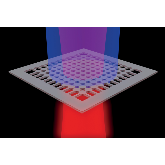
(en anglais) Self-assembly of Si- and SiGe-based dielectric Mie resonators via templated solid-state dewetting
C2N - Site Marcoussis, C2N site Marcoussis, salle R. Planel, MarcoussisSéminaires
Dielectric Mie resonators have attracted a great deal of attention over the past few years thanks to
their remarkable capabilities in manipulating light propagation at the nanoscale1,2,3. However, the practical
implementation of technological products is still elusive. Important limits are the absence of a high-performing
material and a fabrication method that can be easily integrated into modern micro-electronic devices at
affordable costs. Here, we provide theoretical and experimental evidence of solid state dewetting of ultra-thin
silicon and silicon-germanium films on insulators as an alternative fabrication method and semiconductor
material for dielectric Mie resonator applications4-7. These dielectric resonant particles can be obtained over
very large surfaces4 on arbitrary silica substrates5. Remarkably, this self-assembly process is independent on
the sample size. Furthermore, the Si(Ge) islands can be precisely organised in uniform arrays and complex
oligomers arrangements6 featuring low size dispersion. Their composition profile can be controlled a posteriori
via a Ge condensation process to form core-shell Si/SiGe islands7,8 and their diffusion spectrum can be
electrically tuned by changing the refractive index of the environment. As an example, we demonstrate SiGebased
Mie resonator arrays functioning as colour pass-band filters across the full visible spectral range9. The
filters function both in transmission and diffusion and are fabricated using a methodology compatible with CMOS
technology. We note that the use of SiGe-based alloys in novel electronic devices, such as FET and CMOS
transistors, is nowadays extremely important. Because of this, opening the field of dielectric MRs to
SiGe-based semiconductor alloys is an important step forward towards the integration of photonics with
electronic devices.

(en anglais) Group IV compounds and tunable index silicon nitride for multiplatform integrated photonics
C2N - Site Marcoussis, C2N site Marcoussis, salle R. Planel, MarcoussisSéminaires
Over the last decade, Silicon Photonics has established itself as a mature technology for the fabrication of low-cost, scalable integrated optical components. Silicon-On-Insulator (SOI) has been widely accepted as the ideal fabrication platform for silicon photonics components, allowing the implementation of high-index contrast waveguides using CMOS-compatible processes. A wide range of highly performing SOI-devices aimed at applications for the next-generation optical networking have already been demonstrated, such as ultra-low loss waveguides, optical filters, high-speed optical transceivers, as well as the components for all-optical signal processing. Nevertheless, to increase circuit density and functionality, a range of materials are required to enable back-end-of-line (BEOL) fabrication of multilayer waveguiding systems and associated components such as light sources, modulators and detectors. We demonstrate a range of techniques and deposition methods leading to the fabrication of components such as Ge/SiGe electro-absorption modulators or BEOL SiN waveguides enhancing the platform capability for applications such as temperature insensitive CWDM, all optical signal processing through enhanced non-linear characteristics and suspended devices for sensing applications.

(en anglais) Exploring the formation of nanomaterials in liquids through direct imaging
C2N - Site Marcoussis, C2N site Marcoussis, salle R. Planel, MarcoussisSéminaires
Nanostructures can be defined and formed through “bottom-up” processes such as assembly of nanoscale bodies or “top-down” processes such as nanoscale etching. Many of these processes, which are fundamental for materials engineering and fabrication of functional nanodevices, such as assembly of nanoparticles and chemical etching of nanoscale architectures are done in a liquid environment.
Using dynamic in situ TEM imaging [1-3] in liquids, I will describe how nanoparticles form in solution and how these nanoparticles interact with each other. First, I will discuss how phase separation of a solution containing Au ions into solute-rich and solute-poor phases leads to the formation of Au nanocrystal through a pathway that does not follow classical nucleation theory (CNT). Namely, I will show that multiple steps lead to the formation of nuclei from which nanocrystals grow [4]. These steps are: 1) phase separation of a liquid solution into solute-poor and solute-rich phases, from which 2) amorphous nanoparticles which serve as a precursor for nuclei emerges. This is followed by 3) crystallization of these amorphous nanoparticles into crystalline nuclei.
Next, I will highlight the role of intermolecular forces between nanoparticles in solution and describe their role in the assembly of nanostructures from individual nanoparticle building blocks (bottom-up approach) [5]. Specifically, I will show how the balance between repulsive hydration force and attractive van der Waals (vdW) force results in a metastable nanoparticle-pair which promotes their subsequent attachment to each other [5].
Finally, I will conclude by describing our recent work where we track the nanoscale dynamics of wet-etch (top-down approach) processes to shape semiconductor nanomaterials where, through direct imaging, we revealed the intermediate stages of Si wet-etch.
These findings highlight the role of solvent-mediated physical and chemical forces in material synthesis and self-assembly of nanoparticles. Our observations also emphasize the importance of direct nanoscale observation in uncovering previously unknown intermediate states that are pivotal for synthesis and self-assembly.
References:
[1] M. J. Williamson, R. M. Tromp, P. M. Vereecken, R. Hull, F. M. Ross, Nature Materials 2 (2003), p. 532.
[2] H. Zheng, R. Smith, Y. Jun, C. Kisielowski, U. Dahmen, A. P. Alavisatos, Science 324 (2009), p. 1309.
[3] U. Mirsaidov, H. Zheng, D. Bhattacharya, Y. Casana, P. Matsudaira, Proc. Natl. Acad. Sci. U.S.A. 109 (2012), p. 7187.
[4] N. D. Loh, S. Sen, M. Bosman, S. F. Tan, J. Zhong, C. Nijhuis, P. Kral, P. Matsudaira, U. Mirsaidov, Nature Chemistry 9 (2016), p. 77.
[5] U. Anand, J. Lu, N. D Loh, Z. Aabdin, U. Mirsaidov, Nano Lett. 16 (2016), p. 786.
[6] Z. Aabdin, X. M. Xu, S. Sen, U. Anand, P. Kral F. Holsteyns, U. Mirsaidov, Nano Letters 17(5), (2017) p.2953.

(en anglais) Compact Modeling and Circuit Design based on Spin Injection
C2N -Site Orsay, C2n -site Orsay, Orsay CedexSéminaires

(en anglais) Heat Assisted Magnetic Recording Technology – Background, Status and Future
C2N -Site Orsay, C2n -site Orsay, Orsay CedexSéminaires
Heat-assisted magnetic recording (HAMR) media requirements and challenges to extend the areal density (AD) beyond 1.4 Tb/in2 [1] will be discussed. Industry research efforts started in 2000 and Hard Disk Drives (HDD) with capacities beyond 10 Terra-Bytes (TB) per disk drive are expected in 2018 [2]. Key progress efforts beyond recording media are related to read-write heads, head-disk interface (HDI) and channels. Today’s channels allow experimental bit-error rates (BER) down to 10-2 [1].
Todays HAMR media are based on granular high magnetic anisotropy chemically ordered, well textured and chemically isolated L10 FePtX-Y films of about 12 nm average thickness. This is achievable by sputter co-deposition of FePt with grain segregants, Y, like C, BN, SiO2 or TiO2 (carbides, nitrides, oxides). Such segregants laterally exchange-decouple grains and make them permanent magnets with up- or down orientation. Six to ten of such grains form one bit with either up (=1) or down (=0) orientation.
Key ongoing progress efforts include average grain diameter <D> reduction from 8 to 4 nm, grain diameter distribution reduction D/D from 20 to 10 % and Curie temperature distributions TC/TC below 3%. Research and development efforts are adjusting / optimizing TC to the available near field transducer (NFT) laser heat power by doping FePt with Cu or Ni. Thin seed layers like 10 nm thick fcc MgO (100) are important to facilitate the formation of well-oriented grains with high chemical ordering and proper perpendicular magnetic anisotropy Ku > 5.107 erg/cm3 [3]. All this is expected to increase AD up to about 4 Tb/in2 [3]. Other, primarily modeling efforts, predict at least 10 Tb/in2 AD HAMR technology, e.g. based on exchange coupled continuous ECC media, which will also be highlighted.
[1] Ganping Ju et al., IEEE Trans Mag. 51, 3201709 (2015)
[2] Mark Re, Seagate (2016)
[3] D. Weller et al., pss A, 210, 1245, (2013) & D. Weller et al., IEEE Trans Mag 50, 3100108
(2014)

(en anglais) Single electron pumps for the revision of the SI unit Ampere
C2N -Site Orsay, C2n -site Orsay, Orsay CedexSéminaires
In 2018 the General Conference on Weights and Measures will revise the International System of Units (the SI). In the "New SI" four
of the SI base units, the kilogram, the ampere, the kelvin and the mole, will be redefined in terms of fixed values of four natural constants,
namely the Planck constant h, the elementary charge e, the Boltzmann constant kB, and the Avogadro constant NA.
By fixing the value of e the base unit ampere can be directly realized by so-called single electron pumps emitting a single electron at a
repetition frequency f to generate the quantized current I = ef.The talk will focus on the present state of single electron pumps for the
direct representation of a the “new” ampere.

Étude et conception d’antennes à base de métasurfaces destinées aux applications spatiales et aéronautiques
C2N -Site Orsay, C2n -site Orsay, Orsay CedexSéminaires
Cette thèse a pour but de mettre en avant les récentes avancées dans le domaine des métasurfaces. Ces structures ont été utilisées dans le but d’améliorer les performances des antennes classiques ou de concevoir de nouveaux concepts d’antenne. Les travaux menés s’inscrivent dans le cadre d’une collaboration avec des partenaires industriels qui sont Airbus Safran Lunchers, Airbus Group Innovations et le CNES. La thèse est organisée en deux parties. La première partie est consacrée aux métasurfaces utilisées comme des surfaces partiellement réfléchissantes (SPR) pour concevoir des antennes à cavité Fabry-Perot. Un modèle analytique permettant de prédire le dépointage du faisceau d’antenne par une modulation de la phase sur la SPR a été développé. Ensuite, un nouveau concept de métasurface permettant de réaliser du dépointage de faisceau est proposé. Il consiste à appliquer un gradient de phase en faisant varier l’indice effectif le long du substrat diélectrique de la SPR. La deuxième partie de cette thèse est quant à elle consacrée à la conception d’une métasurface active permettant d’émuler plusieurs fonctions. Dans un premier temps, la métasurface est utilisée comme un réflecteur présentant une reconfigurabilité fréquentielle et angulaire. Ensuite cette métasurface est utilisée comme polariseur reconfigurable où une polarisation linéaire de l'onde incidente est convertie en polarisation circulaire. Enfin, la dernière étude concerne l’utilisation de la métasurface active pour la réalisation d’une antenne à réflecteur cylindro-parabolique et à réflecteur dièdre reconfigurables.