

Abstract
Silicon photonics on-chip spectrometers are finding important applications in medical diagnostics, pollution monitoring, and astrophysics. Spatial heterodyne Fourier transform spectrometers (SHFTSs) provide a particularly interesting architecture with a powerful passive error correction capability and high spectral resolution. Despite having an intrinsically large optical throughput (étendue, also referred to as Jacquinot’s advantage), state-of-the-art silicon SHFTSs have not exploited this advantage yet. Here, we propose and experimentally demonstrate for the first time, to the best of our knowledge, an SHFTS implementing a wide-area light collection system simultaneously feeding an array of 16 interferometers, with an input aperture as large as 90µm×60µm formed by a two-way-fed grating coupler. This is one order of magnitude are increase compared with state-of-the-art Si SHFTs. We experimentally demonstrate 85 pm spectral resolution, 600 pm bandwidth, comparable with the state-of-the-art, while achieving a remarkable 13 dB étendue increase, compared state-of-the-art solutions which use conventional grating coupler input. The SHFTS was fabricated using 193 nm deep-UV optical lithography and integrates a large-size input aperture with an interferometer array and monolithic Ge photodetectors, in a 4.5mm2 footprint.
Miniaturized silicon photonics on-chip spectrometers have been identified as an enabling tool for a wide range of applications, including medical diagnostics, biological and environmental monitoring, astrophysics and planetary science, to name a few. In integrated photonic spectrometers, light is collected and processed with a dispersive or a Fourier-transform device. Dispersive devices, e.g. arrayed waveguide gratings (AWGs) and waveguide echelle gratings, have a single input waveguide, limiting the étendue, thus compromising the achievable signal-to-noise ratio. In addition, dispersive elements are quite sensitive to fabrication imperfections. Conversely, Fourier transform circuits benefit from an intrinsically large étendue, i.e., the Jacquinot’s advantage. A particularly promising architecture for miniaturized on-chip Fourier transform circuits is the spatial heterodyne Fourier transform spectrometer (SHFTS). SHFTS relies on an array of Mach–Zehnder interferometers (MZIs) with a linearly increasing optical path length imbalance, to form a spatial interferogram from which the input spectrum is retrieved. SHFTS allows passive calibration techniques to correct amplitude and phase errors due to fabrication imperfections and to achieve a high spectral resolution both in the near-IR and the mid-IR. SHFTS also provide multi-aperture light collection systems that allow increasing the light collection area substantially. However, silicon photonics on-chip SHFTSs reported to date have not yet exploited this large aperture advantage. State-of-the-art SHFTS demonstrations use single-waveguide input and power splitting trees or multiple inputs that are accessed separately, one by one.
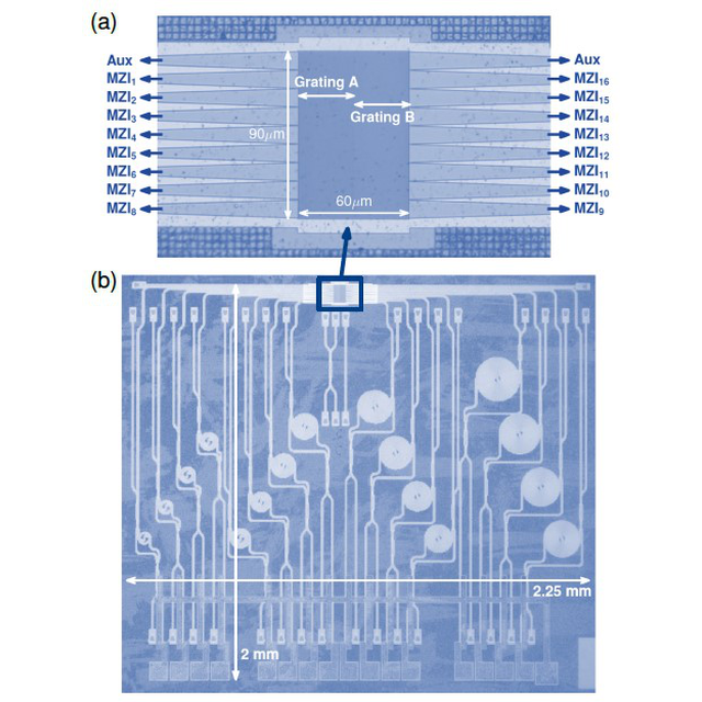
Here, we propose and experimentally demonstrate a novel silicon on-chip SHFTS exploiting the Jacquinot’s advantage, implementing on a wide-area collecting input formed by two grating couplers, side by side [Fig. 1(a)]. One grating is designed for a positive coupling angle θ and the other for a negative angle −θ. Light illuminating the collecting surface is redirected in the chip plane in opposite directions by respective gratings. This two-way-fed grating geometry, which was originally proposed to improve the bandwidth of fiber-chip couplers, is used here to increase the light collecting surface and the number of waveguides fed simultaneously. Based on this approach, we fabricate a SHFTS using 193 nm deep-UV lithography. The input interface, with a surface of 90 µm × 60 µm, simultaneously feeds 16 MZIs, eight on each side. The output of the MZIs is read out with monolithically integrated germanium photodetectors. The deep-UV fabrication and monolithic integration with Ge photodetectors shown here open new perspectives for large-volume fabrication of on-chip SHFTSs.
We experimentally show a resolution of 85 pm with a ∼13 dB étendue improvement for a wide-area input beam with a radius of 0.5 mm, compared with a conventional surface grating coupler (20 × 20 µm2 size). The large étendue of the proposed configuration and the powerful phase and amplitude corrections provided by the pseudoinverse technique allowed demonstration of 85 pm resolution using wide-area input aperture and integrated photodetectors, with no significant performance degradation compared to individual illumination of each MZI and read out with external photodetectors. These results open a new route to large-volume production of miniaturized silicon photonic on-chip spectrometers exploiting the Jacquinot’s advantage, which can be particularly interesting for sensing applications in embarked systems where weight, robustness, and étendue are key parameters.
References
Optics Letters Vol. 46, Issue 6, pp. 1341-1344 (2021)
DOI : https://doi.org/10.1364/OL.418278
Affiliations
Thi Thuy Duong Dinh1,*, David González-Andrade2, Miguel Montesinos Ballester1, Lucas Deniel1, Cécilia Dupré3, Betrand Szelag3, Xavier Le Roux1, Eric Cassan1, Delphine Marris-Morini1, Laurent Vivien1, Pavel Cheben4,5, Aitor V. Velasco2, et Carlos Alonso-Ramos1
1Center for Nanosciences and Nanotechnologies, CNRS, University Paris-Saclay, Palaiseau 91120, France
2Instituto de Óptica Daza de Valdés, Consejo Superior de Investigaciones Científicas (CSIC), Madrid 28006, Spain
3University Grenoble Alpes and CEA, LETI, Minatec Campus, F-38054 Grenoble, Grenoble Cedex, France
4National Research Council Canada, 1200 Montreal Road, Bldg. M50, Ottawa, Ontario K1A 0R6, Canada
5Center for Research in Photonics, University of Ottawa, Ottawa, Ontario K1N 6N5, Canada
Contact
thi-thuy-duong.dinh@c2n.upsaclay.fr
Illustration
Fig. 1. Optical images of: (a) wide-area two-way-fed input grating coupler, and (b) complete SHFTS device, comprising the wide-area coupler, 16 MZIs with linearly increasing optical path length imbalance up to 7.5 mm, and integrated Ge photodetectors.

