Thanks to material and photonic scientists, two groups from C2N have demonstrated the potential of Yttria-Stabilized Zirconia (YSZ) oxide for photonic applications.
Despite the great progress achieved in silicon photonics the last decade, devices functionalities are still limited by the indirect bandgap and centrosymmetric structure of the semiconductor. As a complementary platform, the hybrid integration of complex oxides has been considered due to the large panel of their properties, interesting for telecommunication, sensors or quantum optics to name few applications.
The lattice matching at the oxides/silicon interface, needed for a high quality of integration, can be ensured with an Yttria-Stabilized Zirconia (YSZ) transition layer. Even if YSZ oxide is well known as an electrolyte for batteries or as a buffer layer in thin film form, it has never been characterized for integrated optics.
Scientists from the Centre de Nanosciences et de Nanotechnologies - C2N (CNRS/Univ. Paris-Sud-Univ. Paris-Saclay), demonstrated the potential of YSZ for photonic applications. The study and optimization of Pulsed-Laser Deposition (PLD) of YSZ on sapphire substrate allowed the growth of high quality thin film. The structural characterization by X-Ray Diffraction (XRD) and Transmission Electron Microscopy (TEM) revealed that the growth direction is controllable up to a critical thickness of 350 nm. The development of an innovative process of fabrication in cleanroom environment, adapted to the YSZ specifications and to the deposition technique, allowed to build YSZ-based passives photonic devices such as shallow-etched waveguides and grating couplers. Optical characterization in telecom wavelength range (1.3-1.5 µm) revealed propagation losses as low as 2 dB/cm, in the same order of magnitude than the silicon waveguides fabricated in the same facilities. Those results, obtained within the framework of the European project POPSTAR1, have been published in Physical Review Material.
In addition to demonstrate the potential of YSZ in photonic, this study opened the way to the optical nonlinear characterisation of YSZ, whose the first results are very promising. The method and results regarding the growth and fabrication of low-loss YSZ-based waveguides is an important step for the integration of complex oxides in photonic.
1 H2020 European project ERC POPSTAR: Low power consumption silicon optoelectronics based on strain and refractive index engineering
References:
High-quality crystalline yttria-stabilized-zirconia thin layer for photonic applications,
G. Marcaud, S. Matzen, C. Alonso-Ramos, X. Le Roux, M. Berciano, T. Maroutian, G. Agnus, P. Aubert, L. Largeau, V. Pillard, S. Serna, D. Benedikovic, C. Pendenque, E. Cassan, D. Marris-Morini, P. Lecoeur and L. Vivien
Physical Review Materials 2, 035202 (2018)
DOI: https://doi.org/10.1103/PhysRevMaterials.2.035202
- Centre de Nanosciences et de Nanotechnologies – C2N (CNRS / Université Paris-Sud- Université Paris-Saclay)
Contacts:
- Guillaume Marcaud, PhD student at C2N
- Laurent Vivien, CNRS senior researcher
- Sylvia Matzen, Assistant Professor Université Paris-Sud
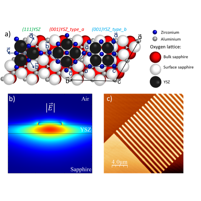
Figures : Crystalline orientation of YSZ on sapphire and YSZ-based passives photonic devices. a) The structural characterization revealed the high quality of YSZ thin films and the three grains orientations with either (111) or (001) growth direction on sapphire substrate. Optimization of Pulsed-Laser Deposition (PLD) allowed to control the growth direction, keeping the crystalline quality, below a critical thickness of 350 nm. b) Optical mode simulation at λ=1550 nm of YSZ-based waveguide (nysz=2.15) on sapphire (nsaph=1.74). The single-mode waveguides allowed the confinement and propagation of quasi-TE mode with an electric field direction in the thin film plane. c) AFM picture of a passive photonic structure made in YSZ thin film: a grating coupler and a taper. © C2N