
PhD defense
Electropreconcentration in nanofluidic devices: predict and experimentally demonstrate stacking/focusing regimes
Centre de Nanosciences et de Nanotechnologies, Amphithéâtre, PalaiseauPhD defense
Jury members:
Pierre Joseph, CR, LAAS-CNRS, Toulouse, Rapporteur
Vincent Senez, DR, IEMN, Lille, Rapporteur
Catherine Perrin, Professeure, Université de Montpellier, Montpellier, Examinatrice
Claude Fermon, SPEC, CEA/Saclay, Saclay, Examinateur
Anne-Marie Haghiri, DR, C2N, CNRS, Palaiseau, Directrice de thèse
Antoine Pallandre, Professeur, Université Paris-Saclay, Orsay, Co-directeur de thèse
Abstract:
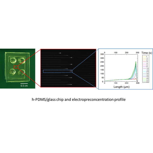
Detection of low concentrated analytes in complex samples is one of the most interesting challenges in bioanalysis. Electropreconcentration based on ion concentration polarization (ICP) effect inside nanofluidic devices appears as an interesting alternative to simultaneously concentrate and detect biomolecules. ICP is induced across nanochannels that play the role of ion-selective filter between microchannels and results in enrichment and depletion zones with high and low conductivity media on opposite sides of the nanochannel where an analyte can focus and therefore concentrate. In this context, the aim of my PhD work is to study preconcentration of chosen analytes in h- PDMS/glass chips incorporating multiple vertical nanochannels. I present 2D numerical simulations of electrophoresis of background electrolyte (BGE) and ionic species inside a micro/nano/fluidic structure using COMSOL Multiphysics® software. These models permits to study first the ICP effect of BGE and then the preconcentration of the analytes. Numerical simulations predict the cathodic stacking (CS) and cathodic focusing (CF) regimes of anionic analytes at nanofluidic interfaces. As part of my experimental work, I studied the role of nanochannel length and width for three model molecules, fluorescein, ovalbumin and hepatitis C DNA. Fluorescein is stacked/focused at the cathode reservoir thanks to its high mobility and the ovalbumin and DNA are preconcentrated at the anode reservoir thanks to their lower mobility.
Find a link in the the attached file below
Lien visio: https://eu.bbcollab.com/guest/21ca1d4365944b4ca57f7bf2a8d4f5ef
Novel concepts for theoretical and applied problems of electromagnetism.
Centre de Nanosciences et de Nanotechnologies, Amphithéâtre, PalaiseauPhD defense
Zoom link: https://cnrs.zoom.us/j/98369602818?pwd=SEYvLzYySnExdEt1aVVrRkQxbmhydz09
Jury members:
Agnès Maître, Professeure, INSP, Paris-Sorbonn, France, Rapporteure & Examinatrice
Jonathan Gratus, MCF HDR, Lancaster University, Royaume-Uni, Rapporteur & Examinateur
Jean-Jacques Greffet, Professeur, IOGS, Université Paris-Saclay, France, Examinateur
Renaud Bachelot, Professeur, Université de Technologie de Troyes, France, Examinateur
Nicolas Boudou, Docteur, LYNRED, France, Invité
Jean-Luc Pelouard, DR, C2N, CNRS, Directeur de thèse
Fabrice Pardo, CR, C2N, CNRS, Co-encadrant
Abstract :
This thesis consists of two parts which, although very different from each other, both belong to the same field: electromagnetism and its modern problems.
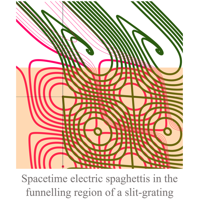
In the first part, an absolute geometrization of the electromagnetic field in spacetime is presented, challenging the claim that the only way to present the electromagnetic field is an abstraction. It is demonstrated that with the absolute topology in spacetime, two scalar invariants are sufficient to describe the electromagnetic field. Particular attention is paid to the case of y-invariant p-polarised field, the topology of which can be represented in 3D spacetime by lines (electric spaghetti), the two scalar invariants then being reduced to one. Unlike the world lines of particles, which are always time-like, these lines transcend the boundary between space and time. This new approach of the electromagnetic field opens up new perspectives both for teaching and for research, in particular the analysis of the topological properties of these absolute structures in spacetime.
The second part is dedicated to a more applied problem, that of the development of nano-absorbers which could become the basis for a new generation of bolometers. In this work, it is demonstrated that thanks to the exceptional properties of plasmonic antennas (total absorption and strong confinement of the electromagnetic field), it is possible to design infrared absorbers whose volume is greatly reduced (several orders of magnitude) compared to those used in current microbolometers. These results pave the way for a major technological breakthrough which, by greatly reducing the thermal capacity of the absorbent, leads to a new sensitivity-speed compromise for bolometers whose performance should then be close to that of cooled photo-detectors.
Zoom link: https://cnrs.zoom.us/j/98369602818?pwd=SEYvLzYySnExdEt1aVVrRkQxbmhydz09
Light amplification and laser emission in electrically driven hybrid III-V semiconductor on SOI nanostructures
Centre de Nanosciences et de Nanotechnologies, Amphithéâtre, PalaiseauPhD defense
Jury Members:
Frederic Gardes, Professeur, Université de Southampton, Rapporteur
Olivier Gauthier-Lafaye, DR, LAAS-CNRS, Rapporteur
Sara Ducci, PU, Université de Paris, Examinatrice
Ségolène Olivier, Docteur, CEA-LETI, Examinatrice
Isabelle Sagnes, DR, C2N-CNRS, Codirectrice de thèse
Fabrice Raineri, PU, Université Côte d’Azur, Directeur de thèse
Abstract:
Exploiting light as a vehicle of the information instead of electrons is thought to be one of the best solutions to go beyond the electrical interconnects limitations. While photonic solutions have already replaced electrical lines for long-distance applications, an optical alternative to the lossy metallic interconnects inside integrated circuits is still missing: particularly, even though silicon waveguides represent a great opportunity to transfer the optical signal throughout the whole chip, active nanophotonic components for low-power applications presenting small footprint, ultra-high driving speed and compatibility with the CMOS-technology, suitable for the on-chip cointegration of photonic and electronic integrated circuits, have not been commercialized yet.
This PhD aimed at developing two fundamental devices we can find inside an integrated photonic circuit: an optical nanoamplifier and a nanolaser source, both relying on an electrically injected hybrid InP on SOI bidimensional Photonic Crystal (2D-PhC). Firstly, we modeled the two devices, demonstrating their efficient electrical injection scheme as well as optical interfacing with a silicon-based passive circuitry, rendering them good candidates for low-power applications. Then, we developed a full technological process flow, fabricating these structures while respecting the limitations imposed by the microelectronic industry. This meticulous task allowed us to validate the designed electrical injection scheme and to demonstrate electrically driven nanolaser, working at room temperature and presenting ultra-low laser threshold power (around 75 µA at 1 V) under an AC electrical bias. Eventually, the limiting technological step was identified and discussed. Its resolution will lead to the demonstration of these nanolasers under a DC electrical signal.
Link :https://univ-cotedazur.zoom.us/j/89349956213?pwd=U1plWlpvMnFPNlBzVTVYT2J2ZTdtUT09
Find a link in the the attached file below
Composants électro-optiques en photonique silicium pour les communications haut-débit et la génération de peignes de fréquences
Centre de Nanosciences et de Nanotechnologies, Amphithéâtre, PalaiseauPhD defense
Jury members:
Anne-Laure BILLABERT, Maître de conférences - HDR, Le CNAM – ESYCOM, Rapporteur
Christophe FINOT, Professeur des universités, Université de Bourgogne, Franche-Comté – ICB, Rapporteur
François MARQUIER, Professeur des universités, École Normale Supérieure, Paris-Saclay, Examinateur
Frédéric GARDES, Professeur associé, Université de Southampton, Examinateur
Stéphane MONFRAY, Ingénieur de recherche, STMicroelectronics, Examinateur
Delphine MARRIS-MORINI, Professeure des universités, Université Paris-Saclay – C2N, Directrice de thèse
Abstract:
La photonique silicium est une technologie de choix pour l’intégration de circuits photoniques complexes sur des puces de quelques mm² pouvant être fabriquées massivement et à faible coût. L’un des enjeux principaux de cette plateforme est la réalisation d’émetteurs-récepteurs optiques miniatures pour assurer les télécommunications haut-débits entre les différents serveurs des centres de données ou datacenters. De nombreuses autres applications ont émergé récemment : la spectroscopie, la radio-sur-fibre ou encore le LIDAR. Pour l’essentiel de ces nouvelles applications, un outil se révèle particulièrement utile : les peignes de fréquences optiques. Ces structures spectrales consistantes en un ensemble de raies laser régulièrement espacées en fréquence et mutuellement cohérentes suscitent un fort intérêt. L’objectif de ma thèse a été d’étudier numériquement et expérimentalement l’aptitude et les performances de modulateurs silicium à la fois dans le cadre des communications numériques hauts-débits à courte portée et de la génération de peignes de fréquence par voie électro-optique.
Une première partie consiste dans l’étude d’un modulateur Mach-Zehnder pour la génération du format PAM-4. Un aspect important de ce type d’application est de pouvoir générer un signal à quatre niveaux sans recourir à des composants électroniques coûteux énergétiquement. D’autre part, il est préférable d’assurer ces transmissions fibrées dans une région spectrale où la dispersion optique est minimale. J’ai ainsi réalisé une démonstration expérimentale d’une génération de signal PAM-4 à 20 Gb/s sans utiliser de convertisseur numérique/analogique et en bande O où la dispersion est proche de 0 ps/nm/km.
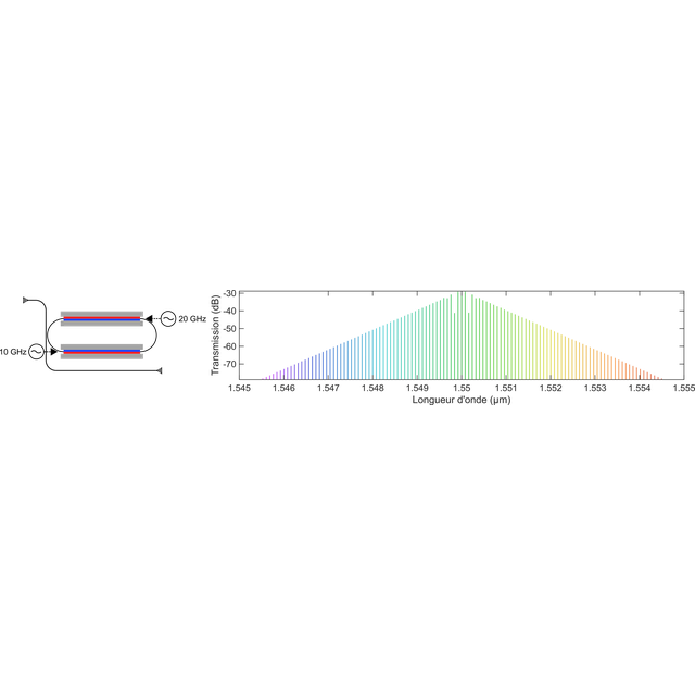
Une seconde partie est dédiée à la génération de peignes de fréquences optiques par des modulateurs en silicium. Les exigences quant aux propriétés des peignes dépendent des applications, mais on peut noter deux caractéristiques généralement désirées : un grand nombre de raie, et une puissance également distribuée parmi les raies (c’est-à-dire un peigne plat). J’ai dans un premier temps étudié deux structures pour la génération de peignes plats basés sur un principe de conversion temps-fréquence à travers une simulation numérique. Dans un second temps j’ai étudié numériquement une structure de modulateur silicium résonnant pour la génération d’un peigne large-bande. Enfin, j’ai réalisé une expérience de spectroscopie à deux peignes à partir de peignes issus de modulateurs silicium, ouvrant la voie aux nouvelles applications de ces dispositifs.
Figure caption: D'après une simulation, un modulateur silicium résonant (à gauche) permettrait la génération d'un peigne de fréquence optique de plus de 100 raies (à droite) par voie électro-optique.
Modeling and simulation of the electrical behavior and the quench effciency of Single-Photon Avalanche Diodes
Centre de Nanosciences et de Nanotechnologies, Amphithéâtre, PalaiseauPhD defense
Jury members:
- Arnaud BOURNEL, Professeur des universités, Université Paris-Saclay, Examinateur.
- Francis CALMON, Professeur des universités, Université de Lyon, INSA, Rapporteur.
- Raphaël CLERC, Professeur des universités, Université Jean Monnet, Rapporteur.
- Anne HEMERYCK, Chargée de recherche, CNRS, Université Toulouse III, Examinatrice.
- Marco PALA, Chargé de recherche, CNRS, Université Paris-Saclay, Directeur de thèse .
- Denis RIDEAU, Docteur-Ingénieur, STMicroelectronics, Encadrant industriel
Abstract:
The development of numerical methods to simulate the electrical behavior and the quench efficiency in SPADs allows guiding the technological improvement of these photodiodes. For this purpose, standard TCAD solvers are often based on deterministic models and carriers are studied in terms of densities, which affects the estimation of the statistical response for a single photon. Therefore, this Ph.D. work aims to improve the simulation of silicon SPADs, focusing on the avalanche dynamics and its quenching description. To achieve this goal, we investigate various device architectures and analyze the main involved physical mechanisms. Furthermore, we assess certain technology trials to enhance the relevant figures of merit and establish the scaling laws. Importantly, a Verilog-A model accounting for the temporal current build-up and its statistics is presented. This physics-based model enables SPICE simulations of circuits and compares favorably with TCAD mixed-mode predictions. Finally, Monte Carlo algorithms are used to compute the photon detection efficiency and the timing response of SPADs. These results correlated with experiments confirm the method’s accuracy, which can be used for modeling future generations of these photonic devices.
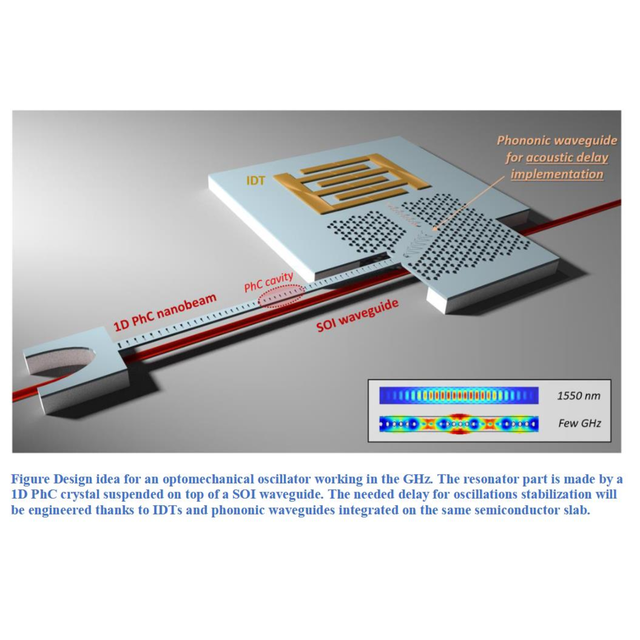
Engineering of an integrated time-delayed microwave OMO: Towards an on-chip acoustic feedback control
Centre de Nanosciences et de Nanotechnologies, Amphithéâtre, PalaiseauPhD defense
Jury members:
Mehdi Alouini, Professeur d’université, Université de Rennes, Rennes, Rapporteur
Sarah Benchabane, HDR, FEMTO-ST, Besançon, Rapporteur
Simon Gröblacher, Professor, TU Delft, The Netherlands, Examinateur
Dries van Thourhout, Professor, Ghent University, Belgium, Examinateur
Rémy Braive, Maître de conférences, Université de Paris, Paris, Membre invité
Isabelle Sagnes, Directrice de recherce, C2N CNRS, Palaiseau, Directrice de thèse
Abstract:
A new generation of oscillators based on optomechanical crystals integrated on photonic circuit could
lead to the generation of high spectral purity and low phase noise signals directly at the micro-wave
frequency. Such device would allow an easy on chip integration at μm scale, where the lack of good
quality and miniaturized source is still a severe issue. Here, the architecture we proposed, uses three
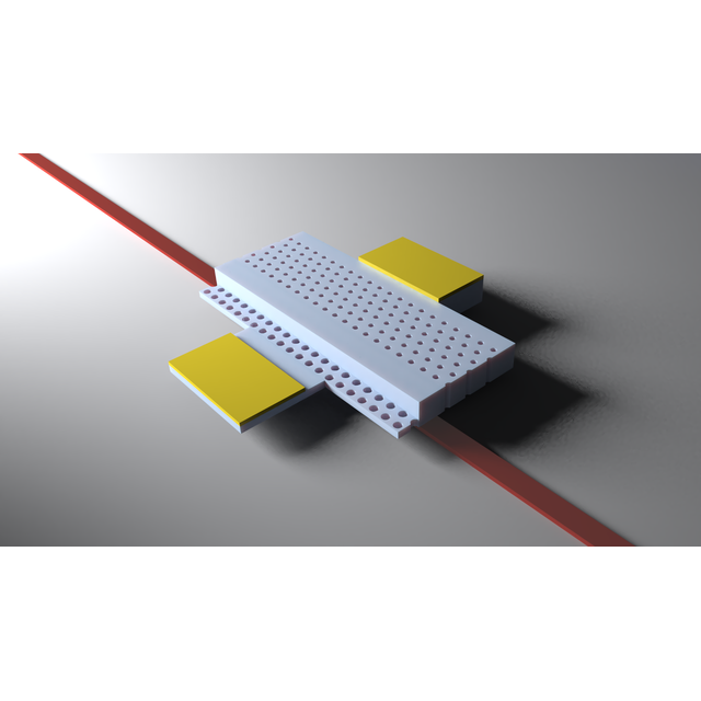
distinct elements (i) a resonator made by a 1D photonic crystal nanobeam suspended over a silicon
waveguide (see fig. 1), sustaining at the same time optical modes around 1.55 μm and mechanical
modes around a few GHz; (ii) interdigitated transducers (IDTs) allowing the acoustical excitation and
thus a full control of the oscillating structure; (iii) a phononic crystal waveguides to engineer the group
velocity of the acoustical waves in order to achieve the desired delay for the stabilization of the
oscillations. These three building blocks composing such a system have been carefully investigated
during this thesis. They will be singularly introduced and discussed in the main body of the manuscript.
Each of them has been studied in depth with simulation, design, nanofabrication and measurements.
It will allow us to show the working principles of these integrated systems as well as the specific
optimization techniques implemented. Once achieved, this will allow us to demonstrate the targeted
objectives for the final implementation in the envisioned complete device. Finally, a first prototype of
a complete system integrating an optomechanical oscillators, an IDT and a phononic waveguide will
be presented, with preliminary results showing the interactions between the different involved
physical domains. The proposed system can be then exploited for potential on-board applications such
as navigation and telecommunication systems, metrology or sensing.
Lien visio: https://u-paris.zoom.us/j/89390229526?pwd=dUxmOXlaTkZjWGp2VFI5UDU3TEY3QT09
Find a clickable link in the attached file below
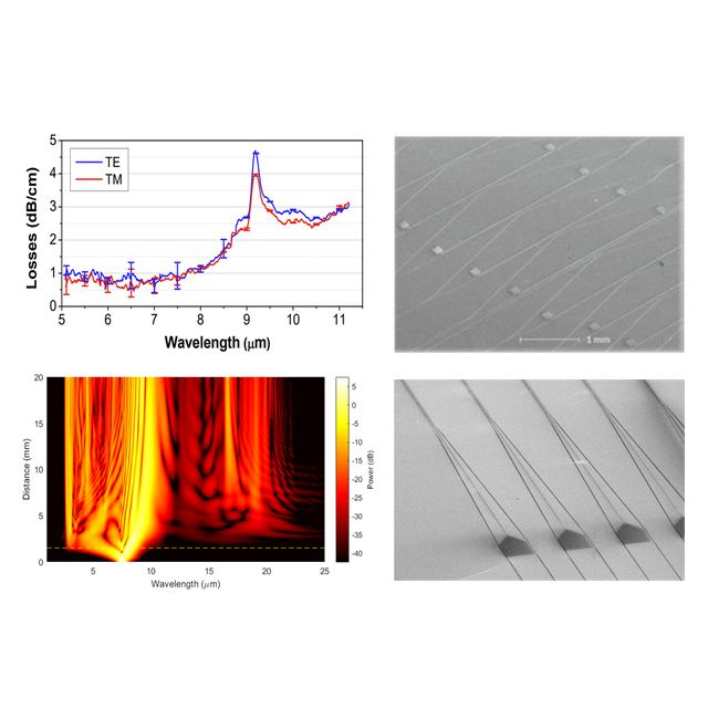
SiGe photonic circuits exploiting nonlinear optics and electro-optic effects in the mid-infrared
Centre de Nanosciences et de Nanotechnologies, Amphithéâtre, PalaiseauPhD defense
Jury members :
Guy Millot (ICB, Dijon)
Jean-Jacques Greffet (IOGS, Palaiseau)
Jean-Baptiste Rodriguez (IES, Montpellier)
Jérôme Faist (ETH, Zurich)
Delphine Marris-Morini (C2N, Palaiseau)
Carlos Alonso-Ramos (C2N, Palaiseau)
Abstract :
The mid-infrared (MIR) spectral range, commonly defined from 2 to 20 µm wavelengths, has attracted a great interest over the past two decades due to its unique characteristics for detection and security purposes. In particular, the fingerprint region (from 3 to 13 µm wavelength) allows a high sensitivity detection of most of molecules due to fundamental molecular vibrational modes that lead to specific absorption lines in this spectral range. During my PhD thesis, I have developed and optimized new fabrication processes in two cleanroom facilities, and also addressed the design, modeling and characterization of three missing functionalities based on thermal-tuning, nonlinear and electro-optic effects, showing a broadband operation in the MIR range.
First, I have demonstrated propagation losses lower than 4.6 dB/cm from 5 to 11 µm wavelength and in both optical polarizations, which are compatible with most of integrated MIR applications. Then, I proposed an integrated spectrometer approach based on a spatial-heterodyne configuration, in which I thermally tuned the path-delay unbalance of a MZI array to overcome the classical tradeoff between resolution, operational bandwidth, and number of interferometric structures required. These results facilitate the development of compact and robust spectrometers operating in the MIR fingerprint region. Next, I demonstrated a supercontinuum generation that spans from 3 to 13 µm wavelength in a 5.5 mm long graded-SiGe waveguide. This demonstration provides a broadband and coherent MIR light by mean of a single device, opening exciting perspectives for the simultaneous detection of multiple molecules. Finally, I experimentally evaluated the free-carrier plasma dispersion effect in a wide MIR range, to later demonstrate an integrated electro-optical modulator operating from 6.4 to 10.7 µm wavelength, showing up to 1.3 dB extinction ratio in current injection regime and 225 MHz modulation bandwidth in carrier depletion. This device is essential to implement synchronous detection and thus significantly improve the sensitivity of integrated detection systems.
In conclusion, this thesis has successfully addressed the development of integrated waveguides and three associated functionalities missing in the literature operating in a wide MIR spectral band. Therefore, this work opens exciting perspectives in a plethora of high-impact applications, paving the way towards the long-term development of compact multi-molecular sensor systems
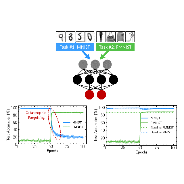
Bio-inspired Continual Learning and Credit Assignment for Neuromorphic Computing
Centre de Nanosciences et de Nanotechnologies, Amphithéâtre, PalaiseauPhD defense
Deep learning algorithms allow computers to perform cognitive tasks ranging from vision to natural language processing with performance comparable to humans. Although these algorithms are conceptually inspired by the brain, their energy consumption is orders of magnitude higher. The reason for this high energy consumption is both architectural and algorithmic. The architecture of computers physically separates the processor and the memory where data is stored. This separation causes particularly intense and energy-intensive data movement for machine learning algorithms, limiting on-board or low-energy budget applications. One solution consists in creating new neuromorphic architectures where the memory is as close as possible to the computation units. However, existing learning algorithms have limitations that make their implementation on neuromorphic chips difficult. In particular, the algorithmic limitations at the heart of this thesis are catastrophic forgetting and non-local credit assignment. Catastrophic forgetting concerns the inability to maintain the performance of a neural network when a new task is learned. Credit assignment in neural networks is performed by Backpropagation. Although efficient, this algorithm is challenging to implement on a neuromorphic chip because it requires two distinct types of computation. These concepts are presented in details in chapter 1 of this thesis. Chapter 2 presents an algorithm inspired by synaptic metaplasticity to reduce catastrophic forgetting in binarized neural networks. Binarized neural networks are artificial neural networks with binary weights and activation, which makes them attractive for neuromorphic applications. The training process of binarized synaptic weights requires hidden variables whose meaning is poorly understood. We show that these hidden variables can be used to consolidate important synapses. The presented consolidation rule is local to the synapse, while being as effective as an established continual learning method of the literature. Chapter 3 deals with the local estimation of the gradient for training. Equilibrium Propagation is a learning algorithm that requires only one type of computation to estimate the gradient. However, scaling it up to complex tasks and deep architectures remains to be demonstrated. In this chapter, resulting from a collaboration with the Mila, we show that a bias in the estimation of the gradient is responsible for this limitation, and we propose a new unbiased estimator that allows Equilibirum propagation to scale up. We also show how to adapt the algorithm to optimize the cross entropy loss instead of the quadratic cost. Finally, we study the case where synaptic connections are asymmetric. These results show that Equilibrium Propagation is a promising algorithm for on-chip learning. Finally, in Chapter 4, we present an architecture to implement ternary synapses using resistive memories based on Hafnium oxide in collaboration with the University of Aix Marseille and CEA-Leti in Grenoble. We adapt a circuit originally intended to implement a binarized neural network by showing that a third synaptic weight value can be encoded when exploiting the low supply voltage regime, which is particularly suitable for on-board applications.The results presented in this thesis show that the joint design of algorithms and computational architectures is crucial for neuromorphic applications.
Link: https://www.youtube.com/watch?v=kCT6AZqZbRE
Find a clickable link in the attached file below
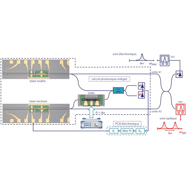
mm-wave generation using optical phase-locked loops for 5G applications
Centre de Nanosciences et de Nanotechnologies, Amphithéâtre, PalaiseauPhD defense
Composition du jury :
Président : Riad Haidar, professeur chargé de cours, Onera, Supoptique, école Polytechnique
Rapportrice : Christelle Aupetit-Berthelemot, professeure, Université de Limoges, XLIM
Rapporteur : Jeremy Witzens, professeur, RWTH Aachen University
Examinateur : Cyril Renaud, professeur, University College London
Examinateur : Guang-hua Duan, docteur, 3SP Technologies
Directeur de thèse : Laurent Vivien, directeur de recherche, CNRS, C2N
Encadrant industriel : Jérôme Bourderionnet, docteur, Thales Research & Technology
Abstract :
One of the key technological issues in the development of future wireless communications network like 5G is the settlement of the new frequencies higher than the classical sub-6 GHz bands, and called millimeter waves (above 30 GHz). Indeed, current frequency bands are close to saturation due to a high number of users and mm-waves represent a very wide unused bandwidth available for 5G and beyond. However, at these frequencies, electronic sources are very expensive, have a high-power consumption and occupy a lot of space, which make them unsuitable for embedded and remote applications. As a replacement optical coherent technology is in first position due to its high compatibility with the already fibered network while requiring very few elements at remote sites, like antennas for instance. Furthermore, the maturity level reached by photonic integrated circuits is now at a decisive moment when they can be used massively within coherent transmission components. This being combined with a downscale of antenna size, due to lower wavelength in millimeter wave, allows new architectures to introduce beamforming and spatial division multiplexing to increase network fronthaul capacity.
Among all optically assisted millimeter wave generation methods the one we deal with in this work is optical phase-locked loop, which compatibility with standardized photonic integrated circuits is also investigated. The working principle relies on an electronic feedback loop making optical phase variations of two independent lasers correlated, and their resulting beat note being then artificially coherent. Thus, the latter is very easy to use in order operate optically assisted frequency up- and down-conversion of a millimeter wave signal. This method benefits from strong assets like its high available optical power and its flexibility toward complex photonics architectures which makes it very suitable to supply photonic integrated circuits dedicated to signal processing, as beamforming networks for instance.
In this work we developed an optical phase lock loop based on commercially available fibered components in order to demonstrate the viability of using semiconductor lasers for coherent applications. This loop has then be implemented in several transmission schemes in the K-band (20-30 GHz) for future 5G experiments, all within the blueSPACE European project. This has led us to investigate the effect of the loop phase noise on QAM modulation formats and OFDM method, both being standards for 5G and beyond. In parallel we designed an optical phase lock loop photonic integrated circuit, which fabrication has been subcontracted to a commercial indium phosphide foundry, in order to evaluate the maturity of the process towards high complexity devices. This semi-industrial approach is validated by state-of-the-art performances for that kind of circuits.
Thèse soutenue en français
Link: https://us02web.zoom.us/j/87121400526?pwd=NjBvSDRNV2xLWnhHSXVaVk5SUGM2Zz09
Passcode: 352864
Find a clickable link in the attached file below
Légende : Description of the designed optical phase-locked loop implemented on an indium phosphide photonic integrated ciruit and delivering a locked beating tone in the mm-wave frequency range.
Nonlinear optics for silicon photonics
Centre de Nanosciences et de Nanotechnologies, Amphithéâtre, PalaiseauPhD defense
Jury members :
Camille-Sophie Brès, Associate professor, EPFL : Rapporteure, examinatrice
Arnaud Mussot, Professeur des universités, Université de Lille : Rapporteur, examinateur
Béatrice Dagens, Directrice de recherche, C2N : Examinateur
Bart Kuyken, Associate professeur, Université de Ghent : Examinateur
Thibaut Sylvestre, Directeur de recherche, Université Bourgigne Franche-Comté : Examinateur
Sébastien Tanzilli, Directeur de recherche, Université Côte d'Azur : Examinateur
Quentin Wilmart, Ingénieur chercheur, CEA LETI : Invité
Laurent Vivien, Directeur de recherche, Université Paris-Saclay : Directeur de thèse
Abstract :
Nowadays, communication networks are becoming more and more important, with the massive emergence of social networks, "streaming" platforms, or even the "Internet of things" for example. In this context where the demand in terms of communications continues to grow, it is necessary to find new technological solutions to overcome the limitations posed by current systems. The emergence of silicon photonics meets all the requirements relating to these needs: this technology allows the creation of ultra-fast communication systems (thus making it possible to transmit more data on the same channel) and reduces the energy consumption of the components of the entire transmission chain. In addition, the use of silicon as the basis for these new systems makes it possible to take advantage of the great maturity of manufacturing processes already established in the microelectronics industry.
During my thesis work, I dedicated my efforts to the exploration of nonlinear optical effects in photonic components compatible with silicon technology. The first objective was to study the possibility of exploiting Pockels effect (a second order nonlinear effect) in silicon to produce ultra-fast and power-efficient electro-optical modulators. Due to the centro-symmetry of the crystal lattice of silicon, this effect is absent in this material. The solution envisaged in this work is to apply a stress on the waveguide in order to deform it and therefore break the crystalline symmetry. Thus, Pockels effect becomes theoretically possible. Modulation experiments in static regime as well as in hyper-frequency regime were carried out. The results show the difficulty of separating the different effects responsible for the observed electro-optical modulation. Indeed, semiconductor effects behave similarly to the Pockels effect, making interpretation of experimental results particularly difficult. Numerical models were set up to establish the contribution of each effect in the electro-optical modulation results.
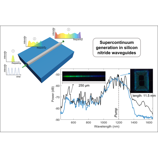
The second axis approached in my thesis concerned the realization of broadband light sources that can work in classic telecommunication windows. Silicon nitride waveguides (a material compatible with silicon technology) were excited with a pulsed laser. By the combination of nonlinear effects and dispersion during propagation, the initial spectrum of the source is drastically broadened, forming what is called a supercontinuum. This type of source is very interesting for producing broadband frequency combs, useful for advanced communication systems, but also in spectroscopy, in imaging, or for chemical and biological sensors for example. In my work, several platforms for manufacturing silicon nitride waveguides were studied. Each platform showed extremely low propagation losses, and their nonlinear properties are compared through pulsed laser light experiments. The generation of supercontinuum as well as two-photon absorption were analyzed in order to conclude on the nonlinear performances of these platforms.
Link: https://us02web.zoom.us/j/87102803431?pwd=T0cxTVVlQUltWGJOOTBTcUNWUzd5UT09
Find a clickable link in the attached file below
