
Séminaires
Et si, la Terre était ailleurs ?
Centre de nanosciences et de nanotechnologies, Amphithéâtre, PalaiseauSéminaires
La science-fiction explore le champ des possibles grâce à des expériences de pensée. Par jeu, demandons-nous avec elle ce que serait devenu l'humanité sur une Terre différente, plus massive par exemple, ou avec des anneaux. Aurions-nous découvert aussi rapidement les lois de la mécanique céleste si la Terre était en orbite autour d'une d'étoile binaire ? Quel impact aurait eu un ciel différent de celui que nous observons quotidiennement ? Finalement, peut-on imaginer quelle serait notre représentation du monde si la Terre était différente ? C'est certainement dans cette capacité à interroger le réel par la pensée, en se posant la languissante question « Et si… ? », que se trouve le lien secret qui unit science et science-fiction.
Roland Lehoucq est astrophysicien au CEA de Saclay. Il est aussi enseignant (Université Paris Cité, ENS Paris-Saclay et Science Po Rennes) et auteur de nombreux ouvrages faisant dialoguer sciences et science-fiction. Depuis 2012, il est président des Utopiales, le festival international de science-fiction de Nantes.

La pollution plastique, des sols aux océans : sources, impacts environnementaux et sanitaires, et efforts internationaux pour l'éliminer.
, c2n amphitheater,Séminaires
Abstract
Alors que les volumes de production de plastiques ne cessent de croître (460 Mt en 2019, double tous les 20 ans), les fuites vers l'environnement suivent la même tendance. Des particules (microplastiques et nanoplastiques) et des substances chimiques sont émises par les plastiques dès leur production et même dès l'extraction des ressources fossiles qui sont à la base de leur fabrication. Les plastiques polluent bien avant de devenir un déchet et sont une menace pour tous les écosystèmes et pour la santé humaine. Les menaces de la pollution plastique pour les écosystèmes marins sont connus depuis une cinquantaine d'années, alors que les recherches sur l'ampleur et les impacts de cette pollution dans les sols sont plus récentes. En raison des milliers de produits chimiques toxiques qu’ils contiennent, les plastiques ont des effets délétères avérés sur le fonctionnement des écosystèmes et sur tous les organismes vivants, y compris sur les humains.
Depuis 2022, un traité international juridiquement contraignant visant à mettre fin à la pollution plastique est en cours de négociations aux Nations Unies. Pour qu’il soit basé sur des faits scientifiques établis sans conflits d’intérêt, les scientifiques pluridisciplinaires travaillant sur la pollution plastiques dans tous les milieux se sont coordonnés dans une Coalition Internationale de Scientifiques, à l’interface entre science et politique. Leurs objectifs sont de partager les connaissances scientifiques, de sensibiliser et alerter les décideurs politiques et le grand public, pour appuyer les États membres qui soutiennent un traité ambitieux et pour contrer les fausses informations.
L'oratrice
Marie-France Dignac est directrice de recherche INRAE. Ses recherches à l'Institut d’Écologie et des Sciences de l'Environnement de Paris concernent le fonctionnement biogéochimique et écologique des sols agricoles, et les impacts des stress anthropiques, comme le changement climatique et les pollutions. Depuis quelques années, ses recherches s'orientent vers les impacts multiples de la pollution plastique des sols agricoles et les conséquences pour les organismes vivants dans les sols et pour l'agriculture. Elle est membre du comité stratégique de la Coalition internationale des scientifiques pour un Traité sur les plastiques efficace et du comité scientifique du GDR Plastiques, environnement, santé.
(en anglais) Efficient spin-photon interfaces with color centers in diamond and silicon
C2N - Centre de Nanosciences et de Nanotechnologies, , PalaiseauSéminaires
The realization of large-scale quantum networks, where distant spin qubits are connected via single photons, offers interesting opportunities for both quantum science and technology. In recent years color centers in various solids emerged as promising candidates for this, providing coherent spin states together with optically active transitions. In this talk, I will give a brief overview of how we can use these centers as spin-photon interfaces. I will discuss recent work investigating the optical properties of the tin-vacancy center in diamond and its integration with nanophotonic structures fabricated in bulk diamond. Finally, I will motivate the interest in developing spin-photon interfaces using silicon as a host material.
(en anglais) EEE-UFFC Distinguished Lecture: Thermodynamics and Phase-field Method of Ferroelectric Crystals with Domains
C2N - Centre de Nanosciences et de Nanotechnologies, , PalaiseauSéminaires
The lecture discusses the thermodynamics and the phase-field method of ferroelectric crystals and their applications to modeling and predicting the stability of domain structures and their responses to mechanical and electric fields. It will start with the basic principles of classical thermodynamics by introducing a modern version of the first law of thermodynamics and applying it to obtain the fundamental equation of thermodynamics for homogeneous ferroelectric crystals. The relations of the fundamental equations of thermodynamics, Landau and fluctuation theories of ferroelectrics, and the thermodynamic properties will then be discussed. It will then be followed by the discussion on the thermodynamics of ferroelectric crystals containing domain structures involving long-range elastic and electrostatic interactions and domain wall energy. The last part of the lecture will be focused on the applications of the phase-field method of ferroelectric domain structures. Examples will be presented to illustrate the application of the phase-field method to interpreting and understanding experimentally observed ferroelectric domain structures and to providing guidance to experimental growth of thin films and characterization to discover new mesoscale domain states of materials, achieve dramatically enhanced properties, and uncover hidden functionality.

Du cycle du carbone au bilan carbone : le LSCE un laboratoire en transition
C2N, , PalaiseauSéminaires
* Présentation en français avec diaporama en anglais.
* RESUME :
La compréhension du cycle du carbone est depuis son origine, l'une des thématiques phares des recherches menées au LSCE. Plusieurs équipes expérimentales et de modélisation s'intéressent à mieux comprendre les mécanismes et les interactions mis en jeu notamment entre les différents reservoirs que sont l'atmosphère, les océans, les écosystèmes. Les équipes ICOS sont notamment en charge de la coordination du service national d'observation ICOS-France pour l'observation et le suivi des concentrations de gaz à effet de serre dans l'atmosphère et du centre thématique atmosphère de l'infrastructure européenne de recherche ICOS (Integrated Carbon Observation System).
Dans un premier temps, je vous décrirai le fonctionnement de ce réseau de mesure quasi opérationnel et je vous présenterai quelques résultats obtenus, puis je replacerai ces travaux dans le contexte plus large de réchauffement climatique actuel et de la nécessité d'évaluer et de limiter l'impact de nos émissions carbone. Dans un second temps, je décrirai le travail piloté pour établir le bilan carbone du LSCE et les résultats obtenus depuis 2019, et je vous présenterai la démarche que nous avons mise en place pour limiter l'impact des activités de recherche du laboratoire.
A propos de Marc DELMOTTE :
Je suis ingénieur de recherche au CNRS / LSCE. Après un doctorat en paléoclimatologie (sur l'analyse des enregistrements issus des glaces polaires), je suis devenu expert dans la mesure d'éléments traces notamment les isotopes puis des gaz à effet de serre. J'ai assuré la coordination technique du service national d’observation des gaz à effet de serre Français pendant une douzaine d'année et je suis toujours impliqué dans ce réseau de mesure. Depuis 5 ans je pilote et j'anime le groupe de travail empreinte écologique du LSCE, et je suis le référent LSCE pour ces questions. Je coordonne notamment le calcul du bilan carbone annuel du LSCE. Je suis également impliqué dans la diffusion es connaissances au sein de la cellule communication du LSCE.
(en anglais) Resonance Antenna for Parametric Excitation of Ultra-Short Spin Waves Based on Voltage-Controlled Magnetic Anisotropy
C2N - Centre de Nanosciences et de Nanotechnologies, , PalaiseauSéminaires
In novel, beyond Von Neumann, computational approaches the use of magnons (or quanta of spin waves) is particularly promising due to the small intrinsic energies of individual magnons (μeV), the possibility of using phase, in addition to magnitude, as a state variable, and the possibility to control the magnon dispersion properties in a magnetic sample by varying the direction and magnitude of the bias magnetic field [1].
However, the use of magnons in advanced and neuromorphic computing is severely limited by the existing linear methods of magnon excitation, which are based on current-driven inductive transducers which have poor energy efficiency due to Ohmic losses, and are unable to effectively excite ultra-short exchange-dominated magnons. Here we propose to use a resonator-like energy-efficient gate, based on the effect of voltage-controlled magnetic anisotropy (VCMA) [2], as a new type of antenna for parametric excitation and reception of exchange-dominated magnons of a submicron wavelength, having a well-defined phase. When a pumping voltage V of a microwave frequency ωp is applied to a resonator-like VCMA gate, the parametric excitation of two short-wavelength counter-propagating half-pumping-frequency magnons ωk and ω-k will occur :
ωp=ωk+ω-k, kp∼0=k+-k . (1)
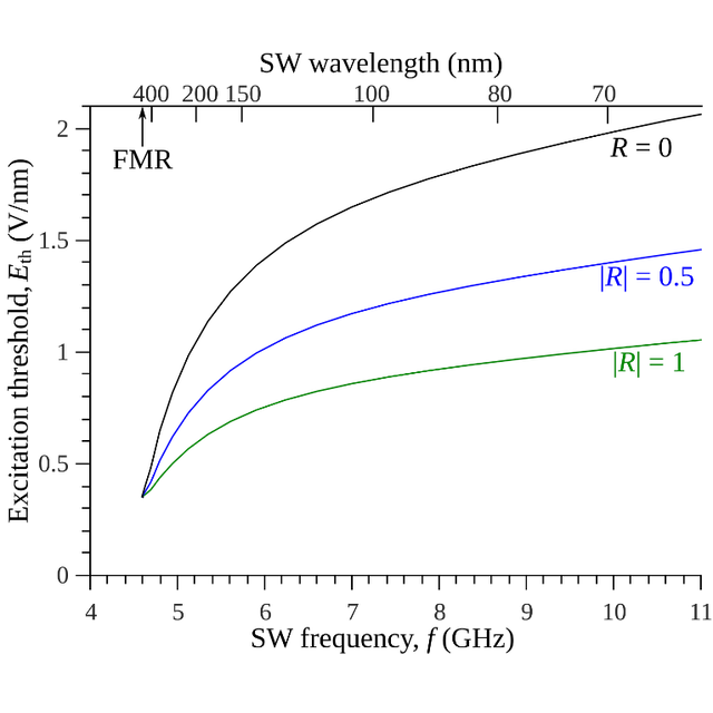
The magnetic anisotropy under the gate will be changed, causing partial reflections of the excited magnons at the both gate boundaries. The excited magnons, then, will have a well-defined phase, that is determined by the phase of the pumping voltage and by the reflection properties of the VCMA resonator. The wavenumber of the excited magnons could be large, and unrelated to the gate size, as it is determined only by the pumping frequency, and the magnon dispersion law ωk . The same resonator-like VCMA gate can also act as a receiver of propagating short-wavelength magnons that will create a standing wave under the gate with double the magnon frequency. This standing wave of the frequency ωp will be detected using a parametric confluence process opposite to the parametric splitting process (1) used for the excitation of magnons at the input VCMA gate. Our calculations show that the reflection of the excited magnons at the gate boundaries reduces the excitation threshold up to two times (in the case of full reflection R=1 ). The calculated excitation threshold for the VCMA gate is presented in Fig. 1. In our calculations we used geometric parameters that are typical for VCMA experiment made on Fe/MgO heterostructures (see e.g. [2, 3]: thickness of the Fe waveguide tFM=1 nm , thickness of dielectric layer tMgO=0.5 nm , waveguide width w=50 nm , and the length of the pumping gate Lg=1 μm . Our preliminary numerical calculation performed for the simplified model of a voltage-biased VCMA gate (see Fig. 1) have demonstrated that the proposed method of parametric excitation and reception of ultra-short-wavelength magnons is realistic, and can be implemented in experiment to generate phase-modulated magnon signals of sub-micron wavelength with high energy efficiency in the GHz and sub-THz frequency ranges.
[1] A. Mahmoud, F. Ciubotaru, F. Vanderveken, A. V. Chumak, S. Hamdioui, C. Adelmann, and S. Cotofana, "Introduction to spin wave computing," Journal of Applied Physics, vol. 128, no. 16, p. 161101, 2020.
[2] P. Khalili Amiri and K. L. Wang, "Voltage-controlled magnetic anisotropy in spintronic devices," SPIN, vol. 02, no. 03, p. 1240002, 2012.
[3] R. Tomasello, R. Verba, V. Lopez-Dominguez, F. Garesci, M. Carpentieri, M. Di Ventra, P. Khalili Amiri, and G. Finocchio, "Antiferromagnetic Parametric Resonance Driven by Voltage-Controlled Magnetic Anisotropy," Physical Review Applied, vol. 17, no. 3, p. 034004, 2022.
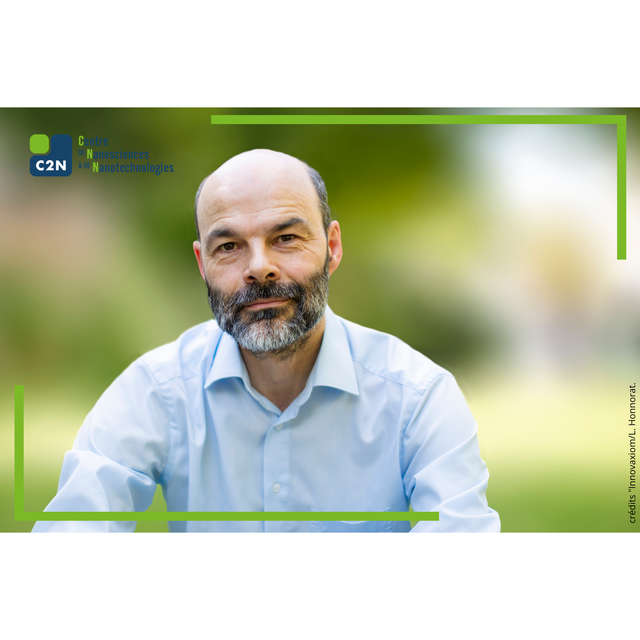
Andrei Slavin received PhD degree in Physics in 1977 from the St. Petersburg Technical University, St. Petersburg, Russia.
Dr. Slavin developed a state-of-the-art theory of spin-torque oscillators, which has numerous applications in the theory of current-driven magnetization dynamics in magnetic nanostructures. His current research support includes multiple grants from the U.S. Army, DARPA, SRC and the National Science Foundation. This research involves international collaborations with leading scientists in many countries, including Germany, Ukraine, France, Italy, and the United States. Dr. Slavin is a frequently invited speaker at international conferences on magnetism around the world.
Andrei Slavin is Fellow of the American Physical Society, Fellow of the IEEE, and Distinguished Professor and Chair of the Physics Department at the Oakland University, Rochester, Michigan, USA.
Figure 1. Calculated threshold (electric field) of parametric excitation of spin waves in a VCMA gate as a function of the spin wave wavelength (top axis) and frequency (bottom axis) for different reflection coefficients R at the gate boundaries.
(en anglais) Bottom-up grown nanostructures: III-V semiconductors and complex oxides.
C2N - Centre de Nanosciences et de Nanotechnologies, , PalaiseauSéminaires
I will present results from our lab on two classes of bottom-up grown nanostructures with applications within quantum technology. First, I will present developments in selective area growth of III-V materials both in terms of scalability and fundamental physics. We have shown how incorporating multiplexing circuits directly on the sample enabled the measurement of hundreds of nominally identical devices during the same measurement run, bringing statistical significance to parameters such as mobility and threshold voltage. We further demonstrate the scalability potential by defining quantum dots in 20 different devices using only three shared crossbar gates. Part of the interest in III-V based nanostructures is due to the interesting physics that arises when they are coupled to superconductors. I will present our results on using quantum interference phenomena to study the symmetries present in III-V/superconductor hybrids.
Finally, I will present results on complex oxide micro-membranes. The interface between materials such as SrTiO3 and LaAlO3 hosts a 2DEG which exhibits signatures of strongly correlated physics, including electron pairing, spin ordering, and superconductivity. However, studying nanodevices in these materials via electron transport is hindered by the failure of traditional fabrication methods. We have recently had success using bottom-up grown SrTiO3/LaAlO3 micro-membranes as the basis for our nanodevices, and I will present preliminary results from these.
Relevant references :
Dāgs Olšteins et al, Nature Communications, 14, 7738 (2023)
Dags Olsteins et al, Nano Letters 24, 6553 (2024)
Ricci Erlandsen et al, Nano Letters 22, 4758 (2022)
Pollutions, Climat et Développement soutenable - Quel cadre de réflexion pour les nouvelles technologies?
c2n amphitheater, ,Séminaires
Abstract
Les trajectoires actuelles de développement ont entraîné des modifications graves, pour certaines irréversibles, du climat et de la biodiversité. Dans cette présentation, nous discuterons des causes et des responsabilités différentiées dans ces changements globaux. nous aborderons également les options évaluées par le GIEC pour parvenir à limiter le réchauffement climatique et les compromis ou synergies de ces options avec les autres enjeux de développement durable.
About the author
Sophie Szopa est directrice de recherche CEA au Laboratoire des Sciences du Climat et de l’Environnement. Spécialiste en chimie de l'atmosphère, elle utilise des modèles numériques pour étudier comment la chimie intervient dans la modification de composition de l’atmosphère et comment cela affecteclimat et qualité de l'air. Elle a coordonné un chapitre sur les composés chimiques à courte durée de vie agissant sur le climat du rapport du GIEC qui évalue les connaissances des bases physiques du changement climatique (AR6-WGI, publié en 2021) et contribué au rapport de synthèse des rapports du 6ème exercice d'évaluation du GIEC paru en mars 2023. Dans le cadre du 7ème cycle d'évaluation du GIEC, elle est également coordonnatrice et auteure du prochain rapport spécial sur le changement climatique et les villes à paraître en 2027. De 2022 à 2024, elle a été vice-présidente en charge du Développement Soutenable de l'Université Paris-Saclay.
Crédit Photo @IPCC
(en anglais) Inherently Selective Atomic Layer Deposition for Optical and Sensor Applications: Microreactor Direct Atomic Layer Processing (DALP™)
C2N - Centre de Nanosciences et de Nanotechnologies, , PalaiseauSéminaires
The integration of additive manufacturing principles with thin film deposition technologies presents significant opportunities for advancing material processing capabilities. While conventional lithography and vapor-phase methods have demonstrated reliable performance, they face fundamental limitations in process flexibility and step reduction. This work explores a novel approach to spatial atomic layer deposition that addresses these constraints. The miniaturization of Spatial Atomic Layer Deposition (SALD) technology introduces specific challenges in gas flow control and precursor delivery. ATLANT 3D presents a micro-nozzle system enabling Direct Atomic Layer Processing (DALP), which achieves localized deposition through precise gas flow confinement within micrometer-scale regions. The system maintains conventional ALD surface chemistry while enabling selective area processing. Initial characterization demonstrates that this approach achieves crystalline thin film formation with quality comparable to conventional ALD methods. The localized nature of the process enables rapid prototyping of materials and processes as well as novel device architectures by reducing the number of required lithography steps. The system demonstrates compatibility with standard ALD precursor chemistries while providing enhanced spatial selectivity.
Experimental validation of this technique has been conducted across several application domains. Temperature sensor fabrication demonstrates sensitivity comparable to conventional methods, while optical applications such as Bragg mirrors exhibit expected reflectivity profiles. The ability to create overlapping depositions enables complex multilayer structures, as evidenced by the formation of ultrathin optical elements. Additional applications in catalysis and microelectronics highlight the versatility of the approach. This work demonstrates the feasibility of miniaturized spatial ALD for selective area processing. The results suggest potential applications in rapid prototyping and novel device architectures, particularly where traditional lithography poses limitations.
(en anglais) Exciting magnetization dynamics with surface acoustic waves: from vortex gyration to spin wave modes of SAFs
C2N, Amphitheater, PalaiseauSéminaires
The elastic coupling between a magnetic film and the substrate is desired in SAW-FMR devices and in magnetoacoustics [1–3] when one harnesses the interaction between a surface acoustic wave (SAW) hosted by a piezoelectric substrate and the magnetization dynamics of a magnetic film on top. We first designed an experiment specifically meant to quantify the magneto-elastic and magneto-rotation field that arise from the mechanical deformations induced by a SAW. For this we prepared magnetic discs possessing a vortex ground state. The discs can be excited either by a remotely generated SAW or by an inductive antenna placed on top of the disc. The vortex dynamics can be measured by magnetic resonance force microscope (MRFM). The antenna has broadband frequency capability and can induce the gyrotropic dynamics of the vortex. The SAWs can also induce this dynamic, provided that the vortex gyration frequency is resonant with that of the SAW [4]. This ability to excite the same dynamics with a classical antenna or with magneto-acoustic interaction allows to quantify the effective magneto-elastic and magneto-rotation fields. It appears that the symmetry of the magneto-acoustic interactions deserved to be revisited. We did such analysis using micromagnetic simulation and analytical calculations. In addition, the symmetry of the coupling can be conveniently studied when studying the coupling of spin waves (SWs) in synthetic antiferromagnets (SAFs) to SAWs [5]. For this we calculated the layer-resolved susceptibility tensor of a SAF, the effective magneto-elastic and magneto-rotation fields associated to a travelling elastic wave, and the power irreversibly transferred by the elastic wave to the magnetic layers. In particular, we showed that in SAF the complementary angular dependencies of the acoustic and optical SW modes makes it possible to excite spin waves for any relative orientation of magnetization and acoustic wavevector.
[1] M. Weiler et al. Phys. Rev. Lett. 106, 117601 (2011).
[2] P. Kuszewski et al. Phys. Rev. Appl. 10, 034036 (2018).
[3] P. Rovillain et al. Phys. Rev. Appl. 18, 064043 (2022).
[4] R. L. Seeger et al. under review, arXiv:2409.05998.
[5] R. L. Seeger et al. Phys. Rev. B. 109, 104416 (2024)
- List of authors and affiliations :
R. L. Seeger(a,b), F. Millo(a), L. La Spina(c), V. Laude(c), A. Bartasyte(c), S. Margueron(c), G. Soares(b) , L. Thevenard(a), C. Gourdon(a), J.-V. Kim(a), C. Chappert(a), A. Solignac(b), G. de Loubens(b), T. Devolder(a)
(a) Centre de Nanosciences et de Nanotechnologies, CNRS, Univ. Paris-Saclay 91120 Palaiseau, France
(b) SPEC, CEA, CNRS, Univ. Paris-Saclay, 91191 Gif-sur-Yvette, France
(c) Univ, de Franche-Comté, CNRS, Institut FEMTO-ST, 26 rue de l’Epitaphe, 25000 Besançon, France
(d) Institut des Nanosciences de Paris, Sorbonne Université,CNRS, UMR 7588, 4 place Jussieu, F-75005 Paris, France
- Bio : Rafael Lopes Seeger holds a Bachelor's and a Master's degree in Physics (2018) from the Federal University of Santa Maria (UFSM), Brazil, and a Ph.D. in Physics (2021) from the Université Grenoble-Alpes at the SPINTEC laboratory in Grenoble, France. Since 2022 he is a postdoctoral researcher working at SPEC (CEA-Saclay ) and C2N (CNRS, Université Paris Saclay) on projects involving magnon-phonon coupling and nonlinear effects in spin waves.
