
Séminaires
(en anglais) Quantum materials by design
C2N, C2N, PalaiseauSéminaires
Abstract :
The electronic properties of a material are dictated by both the composition and arrangement of its atomic lattice. Combining elemental atoms selected from the periodic table in principle provides for infinite varieties of materials to be realized. However, thermodynamic constraints limit which atoms may bond into which symmetry classes; materials may or may not be air sensitive; synthesis conditions may be impractical; impurities and defects may substantially obscure intrinsic electronic properties; and the resulting electron behaviour may not be predictive owing to phenomena such as strong electron interactions, spontaneous magnetic ordering, fermi-surface reconstruction or other effects not captured by single-particle band-structure calculations. In this talk I will explore new approaches to synthesizing quantum materials by augmenting the atomic lattice structure in 2D materials with a superimposed superlattice potential. Artificially engineering lattice potentials provide opportunities to synthesize materials beyond the periodic table, with the ultimate promise to be able to realize and manipulate arbitrary electronic states, by design. Opportunities, and challenges, in this exciting new field will be reviewed, and the prospects for quantum simulation in a solid state platform will be discussed.
About the speaker :
Cory R. Dean is a professor of Physics at Columbia University in the city of New York. He is an expert in the study of two-dimensional (2D) materials where strong correlations lead to novel electronic phases. He received his PhD in physics from McGill University in Montreal where he studied the even-denominator fractional quantum Hall effect in GaAs. As a post-doctoral researcher at Columbia University, he pioneered fabrication techniques for synthesizing layered-heterostructures of van der Waals materials, including the mechanical assembly technique for stacking 2D crystals, and engineering interfacial moire superlattices. Dean’s group has continued to develop novel ways to manipulate the quantum properties of 2D materials, including the development of dynamic superlattice tuning through in-situ layer rotation and pressure, band structure engineering by dielectric patterning, and tunable correlations through applied electric and magnetic fields. He applies these techniques to realize and study exotic quantum phenomenon including superconductivity and magnetism, excitonic superfluids, non-trivial topology, fractionally charged excitations, and non-abelians. Dean has received numerous awards for his discoveries, including : finalist for the Blavatnik National Awards for Young Scientists in 2020, the Presidential Early Career Awards for Scientists and Engineers (PECASE) in 2019, ONR Young Investigator Prize (2017), Alfred P. Sloan Fellowship (2016) David and Lucille Packard Fellowship (2015), Lee Osheroff Richardson Prize (2015), NSF Early Career Award (2014), and IUPAP Junior Scientist Award in Low Temperature Physics (2014). Dean is recognized as being among the top 1% of most highly cited physicists according to clarivate analytics, and holds the distinction of having twice authored a manuscript that was identified by Physics World Magazine as one of the “top ten breakthroughs” of the year.
(en anglais) C2N PhD student seminar
C2N, Amphitheater, PalaiseauSéminaires
- Gaia di Bernardino (C2N Department of Materials) - Growth of phase switching 2D material WSeTe
- Sarra Salhi (C2N Department of Photonics) - Optimized polarization insensitive grating antenna in the SOI platform
- Huber Lam (C2N Department of Photonics) - Optimising the interference of classical and quantum fields
- Zarina Nazyrova (C2N Department of Microsystems) - Development of high > performance piezoelectric MEMS for application to the living field

(en anglais) Memrisitive devices based on Ferroelectric and Topotactic redox oxides
C2N - Centre de Nanosciences et de Nanotechnologies, , PalaiseauSéminaires
Neuromorphic computing seeks to replicate the architecture and information processing mechanisms of the mammalian brain. To achieve this goal, we require new micro or nano-electronic devices capable of electrically mimicking the behavior of biological synapses and neurons. Memristors, characterized by metal/insulator/metal structures, exhibit the ability to alter their electrical resistance between different, usually non-volatile, states. These states can emulate the adaptive, analog synaptic weight of brain synapses, presenting significant potential for the development of bio-inspired devices. Exploring memristive mechanisms beyond the conventional one based on point defect (such as oxygen vacancy) electromigration could lead to devices with enhanced functionalities and lower energy consumption.
In this presentation, I will describe our recent work on the fabrication, characterization, and modeling of various oxide thin film memristive systems. Firstly, I'll focus on ferroelectric perovskite-based devices [1,2]. Drawing from experiments and numerical simulations, we demonstrate that the memristive effect occurs at ferroelectric/metal Schottky interfaces. The interface resistance is modulated by both the direction of ferroelectric polarization and the electromigration of oxygen vacancies, mainly driven by the depolarizing field.
Moving on, I will shift the spotlight to multi-mem devices exhibiting a substantial memcapacitive response. These devices are based on an epitaxial topotactic redox perovskite [3,4]. I'll elaborate on how optimizing the electrical response involves tuning the oxide chemical composition and crystallinity, adjusting the out-of-plane orientation, and fine-tuning the stimulation protocol.
References:
[1] “Key Role of Oxygen-Vacancy Electromigration in the Memristive Response of Ferroelectric Devices”, C. Ferreyra, M. Rengifo, M.J. Sánchez, A.S. Everhardt, B. Noheda, and D. Rubi, Phys. Rev. Appl. 14, 044045 (2020)
[2] “Epitaxial ferroelectric memristors integrated with silicon”, Miguel Rengifo, Myriam H. Aguirre, Martín Sirena, Ulrike Lüders and Diego Rubi, Frontiers in Nanotechnology 4, 1092177 (2022)
[3] “Large memcapacitance and memristance at Nb:SrTiO3/La0.5Sr0.5Mn0.5Co0.5O3-δ topotactic redox interface”, W. Román Acevedo, C. A. M. van den Bosch, M. H. Aguirre, C. Acha, A. Cavallaro, C. Ferreyra, M. J. Sánchez, L. Patrone, A. Aguadero, and D. Rubi, Appl. Phys. Lett. 116, 063502 (2020)
[4] “Optimization of the multi-mem response of topotactic redox La1/2Sr1/2Mn1/2Co1/2O3−x”, W. Román Acevedo, M. H. Aguirre, C. Ferreyra, M.J. Sánchez, M. Rengifo, C. A. M. van den Bosch, A. Aguadero, B. Noheda, D. Rubi, APL Mater. 10, 011111 (2022)
(en anglais) Opto-phononics: Controlling Light and Sound at the Nanoscale
C2N, Amphitheater, PalaiseauSéminaires
Advances in material science and fabrication techniques enabled a new generation of samples with nanometric dimensions where it is possible to confine photons and phonons (GHz-THz frequencies) in a single resonant cavity. In this seminar, I will describe the behavior of a plethora of devices able to control the interactions between light, sound, and charge at the nanoscale. I will introduce some strategies to generate, manipulate, and detect ultra-high frequency acoustic phonons both in the time and spectral domains. The presented results open a new playground in the control of acoustic vibrations in solids and constitute a new platform to study topological effects, quantum phenomena, and thermal transport properties.
Daniel Lanzillotti Kimura obtained his Ph.D. in 2009 from both the Instituto Balseiro in Argentina and the Institute of Nanosciences in Paris. His field of research is nanophoNonics and nanomechanics. Between 2009 and 2015 he was a postdoctoral researcher in the Bariloche Atomic Center in Argentina, the University of California at Berkeley in the US, and the Laboratory for Photonics and Nanostructures in France Since 2015, Daniel Lanzillotti-Kimura is a researcher at the Center for Nanosciences and Nanotechnology of the CNRS in France. He was awarded an ERC Starting Grant and an ERC Consolidator Grant.

(en anglais) Spin waves in curved magnetic shells
C2N - Centre de Nanosciences et de Nanotechnologies, , PalaiseauSéminaires
The exploration of three-dimensional architectures has recently become a focus in several research fields, including the study of ferromagnets and superconductors. Depending on the underlying order parameter and interactions, twisting and bending flat samples into curved shells can lead to many emerging effects when the bending radius is comparable to the system's characteristic length scales. Curvature-induced emergent anisotropies and magnetochiral interactions have been widely studied in ferromagnetic systems, resulting in the discovery of various fascinating phenomena such as stabilizing skyrmions and merons on Gaussian and paraboloid bumps, pinning of domain walls or suppression of the Walker breakdown.
The impact of curvature and three-dimensional shape on magnetization dynamics, namely on the propagation of spin waves, manifests in several aspects: For example, the curvature of magnetic shells can modify the dynamic magnetic pseudo charges. As a result, magneto-chiral symmetry breaking of magnetostatic origin can lead to asymmetric spin-wave dispersion [1], nonreciprocal spatial mode profiles, and strongly modify nonlinear magnetization dynamics [2]. Moreover, a nontrivial topology of three-dimensional magnetic specimens can induce a topological Berry phase of spin waves or impose selection rules on the dynamics of magnetic textures. Furthermore, achiral symmetry breaking, induced, for example, by lowering rotational symmetries, can lead to symmetry-governed splitting of degenerate modes [3,4]. This talk will focus on the aforementioned geometrical effects on magnetization dynamics and introduce numerical techniques for studying spin waves in curved magnetic shells. To this end, the finite-element micromagnetic modeling package TetraX is presented [5], which can efficiently calculate spin-wave dispersions and spatial mode profiles in various curvilinear geometries.
[1] Otálora et al, Phys. Rev. Lett. 117, 227203 (2016)
[2] Körber et al, Phys. Rev. B 106, 014405 (2022)
[3] Körber et al, Phys. Rev. B 104, 184429 (2021)
[4] Körber et al, Phys. Rev. B 105, 184435 (2022)
[5] https://tetrax.readthedocs.org/
(en anglais) Astronomy meets photonics: a unique potential for the next decade
C2N, Amphitheater, PalaiseauSéminaires
New discoveries in astronomy rely primarily on the astronomers' ability to develop and exploit new technologies to process and analyze the very few distant stellar photons collected by telescopes. On the other side photonics has demonstrated, through numerous applications, a strong potential to route and manipulate light, which can be seen as an appealing alternative to classical free space optics. For the last ten years, "astrophotonics" has brought together these two fields and tried to improve on the versatility, robustness and simplification of, otherwise, increasingly complex and bulky instruments onboard the 10m or future 40m telescopes.
In this talk, I will focus on the recent achievements of "photonics for astronomy" mainly in the infrared part of the spectrum. I will review some of the major constrains in observational astrophysics that we are facing when developing new astronomical instrumentation and attempt to give a perspective, based on examples applicable to techniques such as interferometry and coronography, for future synergies that may profoundly impact optical and infrared instrumentation for ground- and space-based astronomy in the upcoming decade.
Keywords: high-angular resolution astronomy, infrared instrumentation, astrophotonics
(en anglais) Advanced numerical methodology for designing passive and active nanophotonic devices
C2N, Amphitheater, PalaiseauSéminaires
In this presentation, I am excited to share with you our cutting-edge optimization approach
for multiobjective metasurface setups. Our method is based on statistical learning, which
utilizes surrogate modeling to predict the behavior of new designs during the optimization
process [1-2]. This approach allows us to rapidly converge to the global set of optimal
solutions while reducing the number of solver calls and iterations compared to traditional
global evolutionary strategies.
We put our optimization approach to the test by optimizing a 3D achromatic metalens with a
numerical aperture greater than 0.5. Our results were remarkable, achieving focusing
efficiencies of almost 50% for three colors (red, green, blue). This achievement sets a new
record for RGB metalens of this kind, and it was accomplished using simple cylindrical
nanopillar geometries that are easier to fabricate than complex freeform geometries [2].
Additionally, we developed a adopted our novel optimization method to consider the
fabrication imperfections relying on the metamodel context [3].
In the second part of my presentation, I will discuss our innovative design strategy to achieve
full phase modulation of light reflected from an arbitrary active metasurface with near-unity
efficiency [4]. We adopted our advanced optimization method and considered the near-field
coupling between strongly resonant pixels and the nonlocal response to maximize the active
beam steering performance. This breakthrough technology has exciting applications in
imaging microscopy, high-resolution image projection, optical communication, and 3D light
detection and ranging (LiDAR).
Overall, our cutting-edge optimization approach together with our innovative design
strategies represent significant breakthroughs in the field of metasurface setups, with the
potential to transform a wide range of applications.
[1] M. Elsawy, et al, «Global optimization of metasurface designs using statistical learning methods», Scientific
Reports, Vol. 9, No. 17918, (2019).
[2] M. Elsawy, et. al, Multiobjective statistical learning optimization of RGB metalens, ACS Photonics, Vol. 8,No. 8,
pp. 2498–2508 (2021).
[3] M. Elsawy, et. al, Optimization of metasurfaces under geometrical uncertainty using statistical learning,
Optics Express 29(19), 29887–29898 (2021).
[4] M. Elsawy, et. al, Universal Active Metasurfaces for Ultimate Wavefront Molding by Manipulating the
Reflection Singularities. Laser Photonics Rev, 2200880, (2023)
keywords: Nanophotonics designs, Multiobjective optimization, Active metasurface, RGB Metalens, Geometrical imperfections
Mahmoud Elsawy is an experienced researcher with a demonstrated history of working in the field of electromagnetic modeling for linear and nonlinear Photonic devices. He received his PhD from the University of Aix-Marseille, France, in 2017, specializing in optics, photonics, and image processing. The topic of his PhD thesis was dedicated to the development of computational models for the design of realistic integrated nonlinear plasmonic waveguides. He spent a year as a postdoctoral researcher at the Institut Fresnel in Marseille, France. After a postdoc at Inria Sophia Antipolis, France, in the field of numerical optimization of nanophotonics, he became a permanent member of the Atlantis project team in December 2020 as an Inria Starting Faculty Position (ISFP) His research activities focus on the modeling and design of innovative passive and programmable metasurface devices.

(en anglais) High performance silicon and silicon metamaterials for integrated photonics
C2N, Amphitheater, PalaiseauSéminaires
Silicon based photonics has been under great scrutiny in recent years due to their potential for making highly compact monolithic integration of multifunctional electronic and photonic devices on the same substrate. The most popular platform is the high index contrast silicon-on-insulator (SOI) system. The high refractive index contrast between the silica cladding and the silicon waveguide core facilitates the confinement and guiding of light in structures within submicron or nanometer dimensions. In addition, the mature silicon microfabrication technology establishes a firm foundation for making low-cost and compact integrated photonic devices. A wide range of active and passive optical devices has been realized on the SOI platform. The applications of these devices can be found in high-speed communications, health industry, chemical and biological analysis, environmental monitoring, optical interconnects, and renewable energy. This talk will focus on the research work by Dr. Ye’s group at Carleton University, ranging from fundamental metamaterial design using subwavelength gratings, polarization rotators and splitters, polarization-insensitive and broadband grating couplers, mode-division multiplexers, multimode couplers, spectral filters, nano-grating antennas, to optical phased arrays.
keywords : Silicon photonics, subwavelength gratings, polarization control, optical antennas, micro-rings/disks
Dr. Winnie Ye is a Fellow of the Engineering Institute of Canada (EIC) and a Full Professor in the Department of Electronics at Carleton University. She was also a Canada Research Chair (Tier II) in Nano-scale IC Design for Reliable Opto-Electronics and Sensors from 2009 to 2021. Her expertise is in silicon photonics and its applications in telecommunications, data communication, biophotonics, and renewable energy. Dr. Ye received her B.Eng., M.A.Sc. and Ph.D degree in Electrical and Computer Engineering from Carleton University and the University of Toronto, respectively. Dr. Ye returned to Carleton as a faculty member in 2009.
(en anglais) femto-second to pico-second laser pulse to switch magnetization
C2N - Centre de Nanosciences et de Nanotechnologies, , PalaiseauSéminaires
During the last decade all-optical ultrafast magnetization switching in magnetic material thin film without the assistance of an applied external magnetic field has been explored [1,2]. It has been shown that femto-second light pulses can induce magnetization reversal in a large variety of magnetic materials [3,4]. However, so far, only certain particular ferrimagnetic thin films exhibit magnetization switching via a single femto-second optical pulse. All optical helicity dependent switching of a ferromagnetic layer could be demonstrated for a low number of pulses [5]. Recently the single-pulse switching of various magnetic material (ferrimagnetic, ferromagnetic) within a magnetic spin-valve structure have been demonstrated. Our experimental study reveals that the magnetization states are determined by spin-polarized currents generated by the light pulse interactions with the GdFeCo layer [6]. A detail study showing how spin-polarized currents are generated and how they interact with a Ferromagnetic (FM) layer can lead to magnetization switching will be presented [7,8]. Magnetization dynamics measurement show that the reversal of the FM layer happens in less than one picosecond which can be modelled [9,10]. Finally single pulse, ultra fast switching could also be observed in Gd free spin valve structure.
[1] C. D. Stanciu, et al Phys. Rev. Lett. 2007, 99, 047601
[2] P. Scheid, et al JMMM 2022 https://doi.org/10.1016/j.jmmm.2022.169596
[3] S. Mangin, et al, Nat. Mater. 2014, 13, 286
[4] C. -H. Lambert, et al Science 2014, 345, 1337
[5] G. Kichin, et al Phys. Rev. App. 12 (2), 024019 2019
[6] S. Iihama et al Adv Matter 1804004 2018
[7] Q. Remy, et al Adv. Sci. 2001996 2020
[8] J. Igarashi, et al Nano. Lett. 20, 12, 8654–8660 2020
[9] S. Iihama et al J. Phys. Soc. Jpn 90, 081009 2021
[10] Q. Remy, et al Nature Com 14 (1), 445 2023
[11] J. Igarashi et al Nature Mat, 114 36 2023
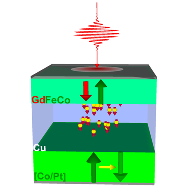
Figure 1 : Sketch of a spin-valve structure used to demonstrate femto-second single pulse switching of each magnetic layer independently. The generation of femto-second spin current is shown to play a major role.
(en anglais) Dynamically Reconfigurable Nanophotonic Devices Enabled by Phase-change Materials
C2N, Amphitheater, PalaiseauSéminaires
A new platform for miniaturized reconfigurable nanophotonics through integration of dielectric, semiconductor, and plasmonic materials with nonvolatile phase-change materials will be discussed. This platform enables reconfigurable photonic building blocks with subwavelength features. Two groups of reconfigurable devices based on integrated photonic structures and metasurfaces along with their unique features for state-of-the-art applications will be discussed. Design, fabrication, and application of this platform for state-of-the-art devices and systems will be covered.
Keywords: Nanophotonics, Phase-change materials, Reconfigurable devices, Metaphotonics
Ali Adibi is the director of Bio and Environmental Sensing Technologies (BEST) and a professor and Joseph M. Pettit chair in the School of Electrical and Computer Engineering, Georgia Institute of Technology. His research group has pioneered several structures in the field of integrated nanophotonics for both information processing and sensing. He is the author of more than 200 journal papers and 450 conference papers. He is the editor-in-chief of the Journal of Nanophotonics, and the nanophotonic program track chair of the Photonics West meeting. He is the recipient of several awards including Presidential Early Career Award for Scientists and Engineers, Packard Fellowship, NSF CAREER Award, and the SPIE Technology Achievement Award. He is also a fellow of Optica, SPIE, and AAAS.