

With the perspective of using two-dimensional materials as growth substrates for opto-electronic devices, a team composed of PhDs, engineers and researchers at C2N is exploring the nucleation of GaN nanostructures on graphene. The growth technique they use is molecular beam epitaxy with a plasma source for nitrogen. As the graphene is exposed to the flow of matter, it takes several tens of minutes before the nucleation of the first GaN nanostructures is detected. The research team and collaborators have clarified what happens during this surprisingly long time. They identified the mechanisms that trigger the nucleation of GaN on this weakly reactive substrate.
The use of a two-dimensional material as a substrate for epitaxial growth is an original and highly attractive concept. Over the recent years, a research team at C2N has been studying a particularly strategic case: the epitaxy of GaN on graphene. The team has already shown that GaN nanowires of high optical quality can grow vertically with a well-defined basal orientation on a graphene substrate. They established the existence of an epitaxial relationship between the two materials but the exact nature of the interface remained an open question. The C2N team is now shedding light on the mechanisms that trigger the nucleation of GaN on graphene, and thus on the binding between the two materials at their interface.
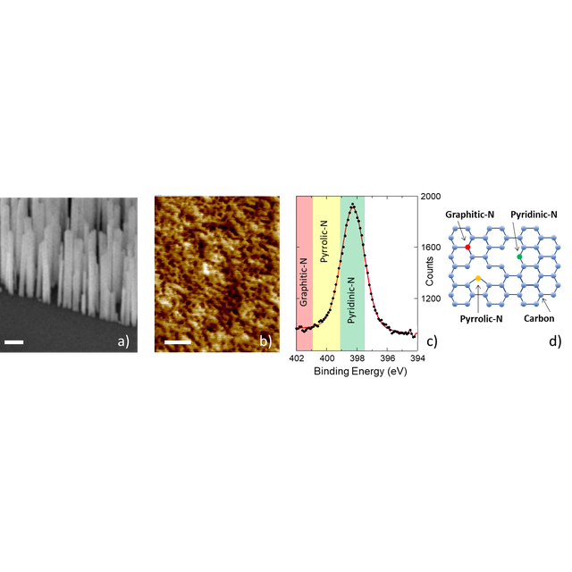
Graphene is prepared by transferring a monolayer of commercial graphene onto a thick layer of amorphous SiO2 obtained by oxidation of a Si wafer. Growth is carried out by molecular beam epitaxy using a plasma source for nitrogen. Using standard conditions and from the exposure of graphene to the fluxes, it takes about 90 min before GaN nuclei start to form. This long "incubation time" is related to the low reactivity of graphene, the surface of which is very stable. The research team has shown that incubation can be shortened by lowering the growth temperature or increasing the incoming fluxes of Ga and N. But the most remarkable observation is that graphene is strongly modified during the incubation period. Indeed, the team evidenced that small pinholes (a few nm in diameter) form into graphene samples exposed to the N plasma. On the surface of these samples, they detected the presence of C-N bonds using X-ray photoelectron spectroscopy. The N1s core level signature corresponds to pyridinic N atoms incorporated in the graphene lattice. Significant changes are also revealed by scanning tunnelling microscopy, in particular point defects.
The research team believes that these pyridinic N atoms act as anchor points for the first GaN nuclei. They propose a plausible growth scenario ; the incubation time would correspond to the following steps: (i) creation of vacancies and then pinholes in the graphene lattice, attachment of N atoms to the pinhole edges and formation of critical GaN nuclei bonded to these first incorporated N atoms.
Two additional arguments support their growth scenario. The dependence of the incubation time on the growth parameters can be modelled very satisfactorily by assuming that this delay time consists of two parts, one that corresponds to the damage of the graphene, the other to overcoming the nucleation barrier. The research team has then applied mechanical stresses with an AFM tip to the GaN nanostructures grown on the graphene layer. They conclude that van der Waals interactions are not sufficient to explain the strong binding between the two materials. This confirms the existence of chemical bonds at the interface.
Références
What triggers epitaxial growth of GaN on graphene ?
Camille Barbier1, Ludovic Largeau1, Noëlle Gogneau1, Laurent Travers1, Christophe David1, Ali Madouri1, Dyhia Tamsaout1, Jean-Christophe Girard1, Guillemin Rodary1, Hervé Montigaud2, Christophe Durand3, Maria Tchernycheva1, Frank Glas1, Jean-Christophe Harmand1
Crystal Growth & Design, 2023, 23 (9), 6517
DOI : 10.1021/acs.cgd.3c00481
Affiliations
1Centre de Nanosciences et de Nanotechnologies - C2N, CNRS, UNIV. PARIS SACLAY, 10 Bld Thomas Gobert, 91120 Palaiseau
2Surface du Verre & Interfaces, UMR 125 CNRS/Saint-Gobain Recherche, 39 quai Lucien Lefranc, BP 135, 93303 Aubervilliers, France
3Université Grenoble Alpes, CEA, Grenoble INP, IRIG, PHELIQS, NPSC, 17 avenue des Martyrs, 38000 Grenoble, France
Contact : Jean-Christophe Harmand
Key words : Epitaxy, graphene, GaN nanostructures
Figure : a) SEM image of GaN nanowires selectively grown on a graphene patch (scale bar 100 nm); nothing grows on the silica next to the patch. b) AFM image of a graphene layer exposed for 60 min to a nitrogen plasma showing that pinholes have formed (scale bar 50 nm). c) XPS analysis of the same surface around the N1s core level revealing the presence of pyridinic nitrogen atoms. The expected positions for the three possible N incorporation sites are shown as coloured rectangles, red for graphitic, yellow for pyrrolic and green for pyridinic. d) Possible incorporation sites of N into a graphene lattice.

