
Soutenance de thèse
(en anglais) Optical phase modulation by Pockels effect in silicon platform
C2N - Centre de Nanosciences et de Nanotechnologies, , PalaiseauSoutenance de thèse
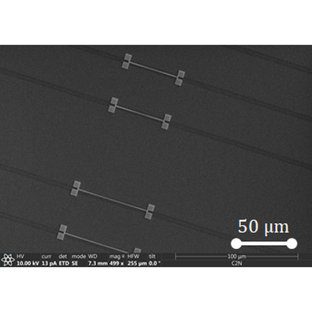
The performance evolution of classical and quantum optical communication networks, computing systems, sensing circuits (including gyroscopes and lidars), as well as integrated circuits, requires the development of pure phase optical modulators compatible with silicon photonics platforms. Addressing this need will directly tackle key challenges in various applications (detection, quantum photonics, optical communications) where silicon photonics could play a transformative role. Silicon's potential for photonics has been recognized to overcome the limitations of interconnect efficiency, while also offering a versatile platform to solve emerging issues in fields such as Lidar and quantum photonics.
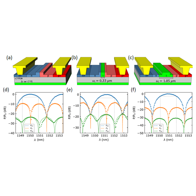
Despite progress in high-performance silicon electro-optical modulators, germanium photodetectors, and III-V lasers on silicon, several challenges remain, including the integration of these elements on a single chip, improving the energy efficiency of optical modulators, and achieving pure phase optical modulation. However, because silicon is a centrosymmetric material, it lacks second-order optical nonlinearities, meaning that there is no inherent Pockels effect or wavelength conversion. To overcome this significant limitation, mechanical stress can be applied to silicon to break its centrosymmetry, thereby inducing second-order nonlinearities. Recent proofs of concept have demonstrated modulation speeds of up to 20 GHz using silicon nitride stress layers deposited by PECVD on silicon.
This thesis focuses on optimizing both the strain-induced Pockels effect and the associated electrode designs. The first part delves into the potential of strained silicon as a platform for achieving the Pockels effect through mechanical stress. Various optical waveguide structure, such as slab and slot waveguides, were explored, but the initial waveguide design from previous work was ultimately the most effective in maximizing the Pockels tensor.
In addition, slow-wave electrodes were proposed as a method to increase electro-optic modulator bandwidth by reducing the velocity mismatch between RF and optical modes. Preliminary results suggest that this method could improve bandwidth, though the fabricated devices—employing silicon nitride stressors—revealed that plasma dispersion effects and carrier absorption mechanisms dominated over the desired Pockels effect. No Pockels effect was detected, primarily due to the strong carrier influence on the modulation process.
Recognizing these limitations, the thesis shifts its focus toward alternative approaches. While silicon nitride stressors have been widely studied, they have proven unsuitable for reliable Pockels modulators due to issues such as surface charges and interface traps. Consequently, the second half of the work explores the study and experimental validation of DC Kerr modulators, which offer a promising solution for pure phase modulation and high-speed applications. The Kerr modulations were quantified through a new experimental protocol designed to separate the contributions of the Kerr effect from plasma dispersion in high-speed modulations. Experimental results showed that the modulation in the studied devices was exclusively due to the DC Kerr effect, enabling the demonstration of an open eye-diagram at 100 Gbps. This advancement sets the stage for future silicon modulators leveraging the DC Kerr effect in high-speed applications.
Nano-ingénierie avancée du transport de la chaleur dans des membranes ultra-minces (2D materials)
C2N - Centre de Nanosciences et de Nanotechnologies, , PalaiseauSoutenance de thèse
Mon sujet de thèse porte sur le transport de chaleur dans des matériaux dit bidimensionnels. Ces matériaux ont des très fortes liaisons dans deux dimensions de l’espace et de très faibles liaisons (de type Van der Waals) dans la troisième dimension. Cette asymétrie a de fortes conséquences en terme de propriétés thermiques. Tout d’abord, la conductivité thermique de ces matériaux va s’en trouver anisotrope. Dans le plan avec les fortes liaisons, celle-ci va être très élevée tandis que dans la direction perpendiculaire, elle peut atteindre les plus petites valeurs observées dans des solides. En outre, le régime de transport de la chaleur dévie du régime classique suivant la loi de Fourier. Ce sont les raisons qui nous ont poussé à s’intéresser aux propriétés thermiques de ces matériaux. Ma thèse s’est décomposée en deux parties. Dans un premier temps, je me suis intéressée au transport thermique dans du hexagonal Boron Nitride (hBN) dont nous avons examiné la conductivité thermique. Nous avons aussi observé un échantillon se trouvant dans un régime où le transport thermique ne suivait plus le modèle classique. Dans un second temps, je me suis intéressée à la possibilité de réaliser de très grands gradients de température à travers des matériaux bidimensionnaux.
Figure : Gradients de température à travers une hétérostructure 2D presentant une déviation du régime classique de la chaleur.
(en anglais) Control of linear and nonlinear resonances in coupled nanoelectromechanical membranes
C2N - Centre de Nanosciences et de Nanotechnologies, , PalaiseauSoutenance de thèse
Micro-and nanoelectromechanical systems (MEMS/NEMS) play a central role in integrated photonics and fundamental physics research. This research focuses on the design, fabrication, and characterization of coupled nano-opto-electromechanical membranes, providing new insights into their linear and nonlinear dynamics.
Key highlights include the development of advanced photonic crystal mirrors for improved optical readouts, enabling precise control and characterization of mechanical eigenmodes in coupled resonators. In the linear regime, interferometric techniques reveal novel phenomena such as CPA-like effects, amplitude annihilation, and phase enhancement. Nonlinear dynamics reveal bistability and multistability, modeled with coupled Duffing oscillators and controlled by innovative feedback strategies.
Expanding to three coupled resonators, the study explores Fano resonances, eigenmode control, and phase locking in both linear and nonlinear regimes, demonstrating the intricate interplay between these effects. These findings open avenues for future research on collective behavior and applications in sensing, low-power modulation, and advanced nonlinear systems.
This work bridges fundamental physics and practical applications, presenting a comprehensive study of coupled resonators that paves the way for innovations in electromechanical technologies.
Legend : Coupled nano-opto-electro-mechanical resonators
(en anglais) Supercontinuum generation in the silicon nitride platform
C2N - Centre de Nanosciences et de Nanotechnologies, , PalaiseauSoutenance de thèse
Nowadays various light sources in different wavelength ranges and serves an important role both for modern industries and people's daily lives. The crucial way towards light source in targeted wavelength range lying on nonlinear optics, which centered on strong light interacting with matters and trigger frequency conversion.
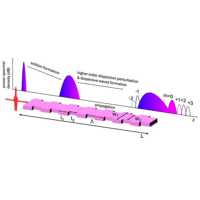
This research focuses on advancing nonlinear optics within silicon photonics to address the growing demand for energy-efficient, integrated, and portable light sources. Silicon photonics, leveraging materials like silicon (Si) and silicon nitride (Si₃N₄), offers key advantages such as high nonlinearity, scalability, and compatibility with semiconductor fabrication processes. The thesis emphasizes the development of supercontinuum generation (SCG) within integrated Si₃N₄ waveguides, aiming to create customizable and power-efficient broadband light sources for applications in medical diagnostics, spectroscopy, and metrology.
Key achievements include:
This work paves the way for fully integrated, on-chip SCG systems, offering tailored spectral broadening for a range of applications in visible and near-infrared wavelengths.
Figure :
Concept of quasi-phase-matched dispersive waves generation in Si3N4 waveguide with group velocity dispersion modulation.
(en anglais) Spin noise spectroscopy of single spins using single detected photons
C2N - Centre de Nanosciences et de Nanotechnologies, , PalaiseauSoutenance de thèse
Quantum emitters capable of high-fidelity and high-rate operation are the cornerstone of photonic quantum technologies, which require increasing precision in the manipulation of single qubits. Emitters that can host a spin are particularly interesting for quantum communication networks and quantum computation, as they exploit the key resource of spin-photon entanglement. In this context, self-assembled semiconductor quantum dots (QDs) have become promising candidates for spin-photon interfaces due to their exceptional optical properties. Nevertheless, short spin coherence times strongly limit the potential of this platform. Better strategies to mitigate the environmental fluctuations and decouple the spin from them are required to improve its performance.
In this regard, Spin Noise Spectroscopy (SNS) has become a key technique to obtain information from spin environments in atomic and solid-state systems via the measurement of polarimetric signals such as Faraday polarization rotation. However, the low signal imprinted by a single spin has limited most SNS implementations to spin ensembles. In this manuscript, we introduce a novel SNS technique based on the measurement of single spins via the detection of single photons. We demonstrate spin noise measurements in the ultrafast regime above the 10 GHz level, breaching traditional bandwidth limitations with unprecedented sensitivity.
Our approach relies on the cavity-enhanced spin-photon interaction, increasing several orders of magnitude polarimetric signals from a single spin. Spin-dependent polarization rotations of the photons reflected from the interface of up to π are observed, allowing for the mapping of spin fluctuations into polarization fluctuations and the efficient optical detection of spin noise mechanisms. Crucially, the SNS signal is mapped into single photons. As a result, correlations can be directly calculated between single photon detection events, dramatically improving the detection bandwidth. Ultimately, the temporal resolution is only limited by the temporal jitter of single-photon detectors.
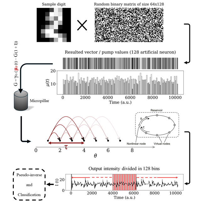
(en anglais) Neuro inspired computing with excitable microlasers
C2N - Centre de Nanosciences et de Nanotechnologies, , PalaiseauSoutenance de thèse

(en anglais) Design, study, and fabrication of coupled cavity arrays for investigating non-hermitian zero-modes
C2N - Centre de Nanosciences et de Nanotechnologies, , PalaiseauSoutenance de thèse
(en anglais) Reconstructing mode profiles of optomechanical crystals by nearfield scanning
C2N - Centre de Nanosciences et de Nanotechnologies, , PalaiseauSoutenance de thèse
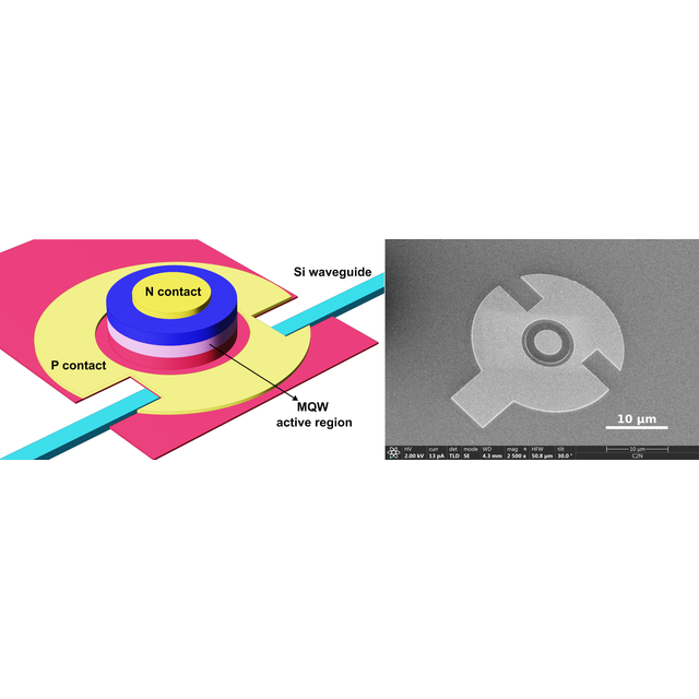
(en anglais) Optical nonlinearities in III-V-on-Si active nanostructures
C2N - Centre de Nanosciences et de Nanotechnologies, , PalaiseauSoutenance de thèse
Hybrid integrated micro- and nanolasers enable efficient light emission at chip scale with reduced power consumption and footprint. Their unique properties make them good candidates for overcoming the limitations of copper-based interconnects. Together with this, the exploitation of their optical nonlinearities has been shown to be effective in the demonstration of nonlinear activation functions in the context of optical neuromorphic computing.
The PhD work regards the design, fabrication and characterisation of InP-on-Si microdisk laser diodes, together with the modelling and characterisation of the latter in the injection locking regime for the implementation as an all-optical activation function. The design is based on numerical simulations to study the electro-optical properties of the laser. In particular, with respect to previous demonstrations, a novel electrical pumping scheme is proposed. The modelling of the device shows the possibility of achieving sub-mW operation in such a configuration, considering a disk of 3.75 μm radius. The fabrication of the devices follows, based on the adhesive bonding of the III-V and SOI sections. Experimental characterisation of the device under DC electrical pumping reports sub-mW operation for the 3.75 μm radius microdisk (390 μA of threshold current at 1.06 V of applied bias). The last part of the thesis is devoted to the study of the nonlinear operation of the microdisk in the injection-locked regime. After the theoretical description of the injected system, two different characterisations are reported at 10 kHz and 2 GHz of modulation, respectively. A saturating, sigmoid and bistable response with μW-scale switching powers is reported in the first case. A clipped GeLU, sigmoid and inverse ELU response are reported in the second case.
Figure : (left) scheme of the III-V on SOI microdisk laser diode. (right) SEM image of the device.
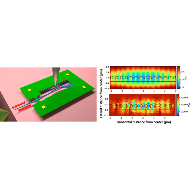
(en anglais) Multimodal one-dimensional photonic crystal cavities
C2N - Centre de Nanosciences et de Nanotechnologies, , PalaiseauSoutenance de thèse
Integrated photonics research focuses its efforts in developing miniaturised and efficient devices for applications in quantum information, metrology and medicine. In this context, photonic crystal cavities occupy a leading position in the integration of photonic structures owning small footprint and tailorable spectral properties. Special attention in recent years is given to photonic crystal cavities consisting of III-V semiconductor materials, as their nonlinear properties are an asset for further development in complex circuitry of coherent states of light through nonlinear interactions.
In this thesis, we present the design, fabrication and experimental characterisation of one-dimensional photonic crystal cavities integrated on silicon on insulator. First, we detail the design of our cavities which is based on the gentle confinement of the field. We show that our design technique allows the design of multimodal as well as single-mode photonic crystal cavities working at telecom window. The introduced design technique is versatile and easily tailorable to devise cavities of different materials, as InGaP, Si, or InP. Then, we detail the fabrication of III-V photonic structures heterogeneously integrated on silicon on insulator. From the adhesive bonding of the two levels to the final integrated device, fabrication process flow is reported and main challenges encountered commented. Fabrication of silicon-based cavities is also reported. Experimental characterisation of the cavities is conduced by measuring the transmission of the samples. We present how to tailor the spectral properties of the cavities through nanometric variation of their geometrical parameters, and comment on some peculiarities of multimodal coupling.
Figure : One-dimensional InGaP photonic crystal cavities integrated on SOI