Soutenance de thèse
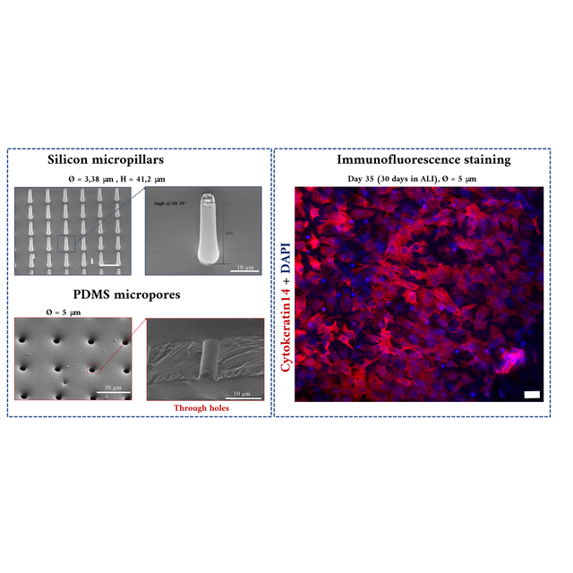
Développement et validation d’un dispositif de culture de cellules épithéliales en interface air-liquide pour la modélisation biomimétique de cavités nasales.
Centre de nanosciences et de nanotechnologies, Amphithéâtre, Palaiseau
Soutenance de thèse
Les technologies organe-sur-puce offrent une approche prometteuse pour reproduire in vitro des modèles physiologiquement pertinents. C’est le cas pour les barrières épithéliales humaines, en particulier pour étudier et prédire le dépôt des médicaments administrés par voie nasale, tout en supprimant le recours aux modèles animaux, tant pour des questions de compatibilité biologique que d’éthique. Cette thèse décrit le développement d'un système destiné à terme à accueillir des cultures de cellules épithéliales respiratoires nasales humaines. Une plateforme microfluidique adaptée aux cultures épithéliales en interface air-liquide (ALI) permettant de tester plusieurs conditions expérimentales parallèlement a été développée. Une stratégie de fabrication reproductible pour obtenir un réseau de neuf membranes microporeuses intégrées dans une seule couche de PDMS et présentant trois différents diamètres de pores (3, 5 et 7 µm) à l'échelle d'un wafer 2 pouces a été mise au point. Le réseau de membranes a été assemblé avec un système fluidique et a permis de tester plusieurs conditions expérimentales au sein d’un même dispositif. La plateforme a été validée avec un modèle de kératinocytes de l'épiderme (HaCaT), montrant une prolifération comparable entre les tailles de pores et une différenciation épithéliale maintenue jusqu'à 30 jours en culture statique et 24 jours sous flux. Cette plateforme constitue ainsi une base non seulement pour le développement ultérieur du modèle biomimétique de cavité nasale, mais également pour l’étude d’autres modèles de barrières épithéliales en interface air-liquide.
Membres du jury :
À gauche: Observations MEB des micropiliers en silicium à haut rapport d’aspect (12), servant au moulage des membranes microporeuses. Images des micropores débouchants après démoulage du PDMS.
Légende figure :
À droite: Expression de la Cytokératine 14 (après 30 jours de cultures cellulaires en ALI), un marqueur spécifique des cellules de la couche basale de l'épiderme.
(en anglais) Identical quantum dot-based single-photon sources
Centre de nanosciences et de nanotechnologies, Amphithéâtre, Palaiseau
Soutenance de thèse
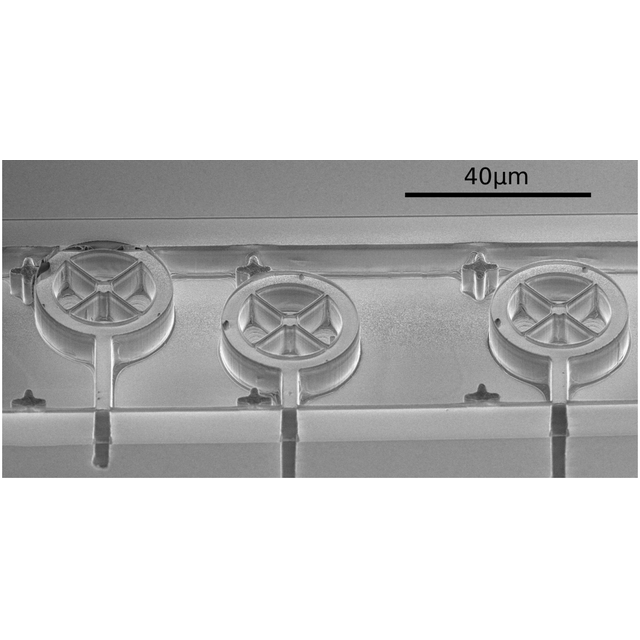
Semiconductor quantum dots embedded in micropillar cavities are bright and deterministic emitters of indistinguishable single photons. Scaling up quantum photonic technologies requires interfering photons emitted from independent sources, which in turn demands perfectly identical emitters. Achieving such reproducibility relies on precise cavity fabrication, robust tuning mechanisms, and environmental noise mitigation.
In this thesis, we address all three of these challenges. We first adjust the micropillar cavity diameters individually and narrow the acceptable spectral range of the QD transitions to fabricate sources with nearly identical optical properties. Secondly, we study the noise affecting our single-photon source and find lower QD density across the grown wafers can reduce the charge noise. Finally, making use of our p-i-n diode structure and a fiber on top of the source, we implement both electrical and strain tuning on the emitters.
We demonstrate state-of-the-art two-photon interference of 88% between remote cavity-embedded QDs. This value is in close agreement with the estimated upper bound of 88.3(1)% , calculated by considering only the individual source Hong–Ou–Mandel interference visibilities and the difference in decay rates between the QDs, demonstrating the near-perfect stability of our emitters. These results mark a critical milestone for the development of multi-source quantum devices and pave the way toward the implementation of scalable quantum networks and photonic quantum computers.
Jury members :
Figure : Scanning electron microscope image of three micropillar single-photon sources.
(en anglais) Control of mid-infrared light dispersion and polarization with SiGe photonics / Contrôle de la dispersion et de la polarisation de la lumière infrarouge moyenne via la photonique SiGe
Centre de nanosciences et de nanotechnologies, Amphithéâtre, Palaiseau
Soutenance de thèse
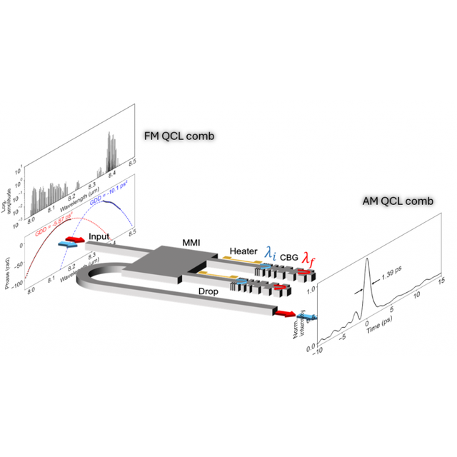
The mid-infrared is a key spectral range for spectroscopy and chemical sensing. Such applications could become accessible to a broad audience through photonic integration. In this context, this thesis explores the use of silicon-germanium (SiGe) photonics to control two properties of quantum cascade lasers (QCLs): dispersion and polarization. First, dispersion control using variable-period Bragg gratings combined with a multimode interferometer enabled the generation of 1.39 ps ultrashort pulses around 8 µm from a QCL frequency comb. Second, a polarization rotator consisting of a mode-evolution waveguide and an asymmetric directional coupler was developed, demonstrating a conversion rate exceeding 88% between 7.5 and 8.9 µm. These achievements constitute essential building blocks for the development of fully integrated spectroscopic systems.
Jury members :
Développement de dispositifs photoniques à base de phosphure de gallium à orientation structurée pour la translation spectrale de peignes de fréquences
Centre de nanosciences et de nanotechnologies, Amphithéâtre, Palaiseau
Soutenance de thèse
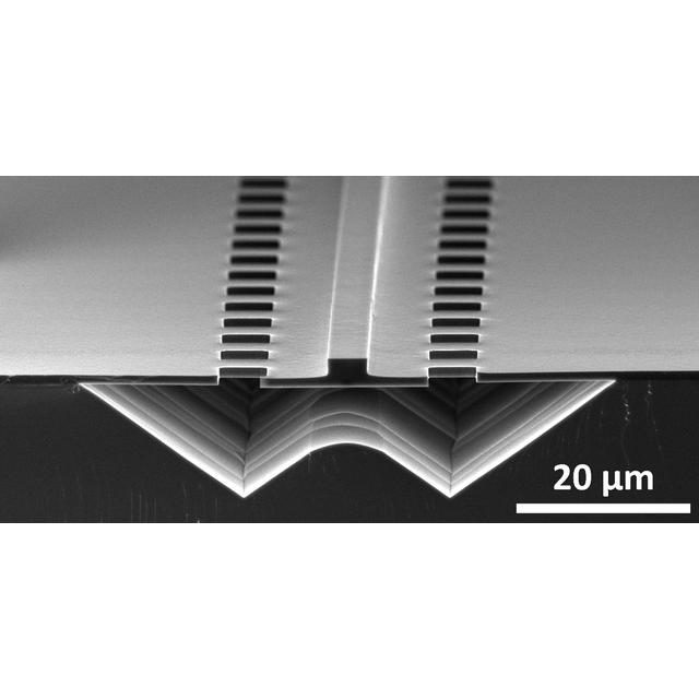
Depuis les travaux réalisés sur les peignes de fréquences optiques en 2005, le développement de la spectroscopie haute résolution a permis d’ouvrir de nouvelles possibilités d’application de l’optique dans divers domaines tels que l’environnement, la santé et la défense. Néanmoins le champ d’application de ces peignes de fréquences optiques reste restreint de par la complexité de leur mise en œuvre. Les premières démonstrations récentes de peignes de fréquences sur puce (microcombs) ont ouvert la voie à de possibles utilisations futures de peignes de fréquences dans nos vies quotidiennes. Cette thèse s’inscrit dans le projet OFCOC (Optical Frequency Combs On a Chip) du PEPR Electronique, dont le but est de former la première source microcomb intégrée, large bande, fiable, robuste et miniaturisée sur une plate-forme exclusivement semi-conductrice en travaillant à la cointégration de deux filières : les ICLs (interband cascade lasers) à base d’antimoine et la plate-forme non-linéaire de GaP. C’est dans ce contexte que ce travail vise à explorer la translation spectrale de peignes de fréquences par des processus non-linéaire d’ordre 2, fonction clef pour le développement de cette technologie. Le premier volet de cette thèse est axé sur l’ingénierie de l’acceptance spectrale de dispositifs à base de phosphure de gallium à orientation structurée (OP-GaP) pour la translation spectrale de peignes de fréquences télécoms et moyen-infrarouge vers la gamme spectrale de détection du silicium par génération de seconde harmonique (SHG) ou génération de somme de fréquences (SFG). Le second volet porte sur la fabrication de guides d’OP-GaP à grande plage spectrale pour la translation de peigne, et sur leur caractérisation linéaire et non-linéaire. Le dernier volet est axé sur la démonstration de la translation spectrale de peignes de fréquences télécoms et moyen-infrarouge vers le spectre visible.
Membres du jury :
Rapporteurs :
Examinateurs/examinatrices :
Encadrants :
Figure : Image SEM de la facette clivée d’un guide OP-GaP suspendu conçu pour la translation large bande de signaux télécoms vers le spectre visible.
(en anglais) Electric-field-assisted phase switching in semiconducting nanowires Contrôle par champ électrique de la structure cristalline de nanofils semi-conducteurs
Centre de nanosciences et de nanotechnologies, , Palaiseau
Soutenance de thèse
Polytypism, namely the existence of different stacking sequences of the crystal planes of the same material, provides a route to heterostructure formation in semiconductor nanowires. In III–V nanowires, such crystal phase heterostructures can be obtained through the controlled stacking of the cubic (zinc blende) and hexagonal (wurtzite) structures. One may thus form crystal phase quantum dots (CPQDs), which are promising building blocks for quantum devices.
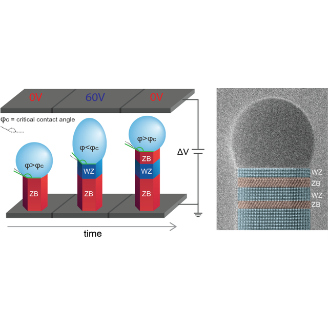
This thesis investigates the precise control of crystal phases in GaAs nanowires for CPQD fabrication using electric-field (E-field) assisted phase switching. Growth is performed by metalorganic chemical vapor deposition in the in situ NanoMAX transmission electron microscope, using specially designed cantilevers that provide a heated substrate and allow one to apply the E-field. The nanowires grow epitaxially in the vapor-liquid-solid mode with a liquid catalyst droplet at their tips. The method consists in changing quasi-instantaneously the shape of the droplet, and therefore its contact angle, by applying the E-field.
A major contribution is the demonstration of reversible crystal phase switching with atomically abrupt interfaces. Crystal phase insertion sizes down to a single monolayer are achieved. Several factors influencing CPQD formation are investigated. In addition to the droplet contact angle, a high enough temperature is found to be another key parameter for wurtzite growth. This is attributed to the temperature-dependent decomposition of metalorganic precursors, which may modify the surface energies of the nanowire facets and consequently affect crystal phase selection. In addition, the polarity of the E-field is found to affect the growth rate. Upon E-field reversal, growth rates become lower or higher than under no E-field. The possible causes of this effect are discussed.
Numerical simulations are used to investigate the effect of the E-field on the geometry of the droplet and to elucidate the mechanism of E-field-induced phase switching. The critical contact angle for phase selection is calculated from a combination of simulations and classical nucleation theory, and is compared with the experiments.
Jury members :
Rapporteure/rapporteur:
Examinateur/examinatrice:
Figure: By applying an electric field (E-field) during the growth of GaAs nanowires, we achieve reversible crystal phase switching between zinc blende (ZB) and wurtzite (WZ). The E-field dynamically deforms the catalyst droplet, reducing its contact angle j below the critical value for WZ formation and thereby triggering the ZB-to-WZ transition with monolayer precision. The TEM image shows a sharp crystal phase heterostructure obtained by this method, with WZ segments formed under E-field.
Lasers GeSn à puits quantiques multiples intégrés sur plateforme GeSnOI : Fonctionnement à température ambiante et en régime continu
Centre de nanosciences et de nanotechnologies, Amphithéâtre, Palaiseau
Soutenance de thèse
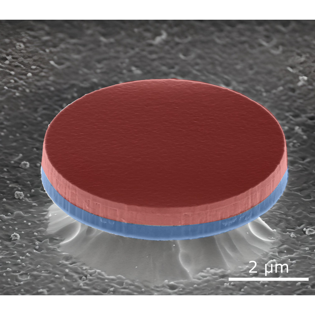
L’intégration de sources lasers sur silicium pour le proche et le moyen infrarouge (de 2 à 5 µm) trouve aujourd’hui un vecteur privilégié dans les alliages de germanium-étain (GeSn). Néanmoins, le développement de ces dispositifs se heurte encore à des verrous technologiques majeurs, limitant leur fonctionnement à température ambiante sous pompage électrique. L'introduction de puits quantiques multiples (MQW) constitue l'une des voies les plus prometteuses pour abaisser le seuil laser et élever la température maximale d’émission. Cependant, le manque de modèles théoriques consolidés et la nécessité historique de croître ces structures sur d’épaisses couches tampons ont, jusqu'à présent, freiné la rupture technologique attendue.
Au cours de ce travail de thèse, des empilements MQW GeSn ont été intégrés pour la première fois sur une plateforme de germanium-étain sur isolant (GeSnOI). Cette technologie innovante, qui a déjà démontré son efficacité sur matériau massif, s'impose à ce jour comme la seule filière ayant permis un fonctionnement laser à température ambiante ou en régime optique continu. Les plateformes GeSnOI offrent des avantages déterminants : un confinement optimal du mode optique au plus près des MQW, la suppression totale de la couche tampon défectueuse, une dissipation thermique efficace, ainsi que l’introduction d’une contrainte en tension au sein de la zone active, favorisant le caractère direct de la structure de bande du GeSn.
Grâce à cette approche, nous démontrons les premiers lasers GeSn MQW fonctionnant à température ambiante, ainsi que les tout premiers lasers MQW opérant sous pompage optique continu. Ces résultats inédits apportent une compréhension nouvelle de la physique et du comportement dynamique de ces composants.
(en anglais) Métaplasticité Bayésienne : l’Incertitude comme Principe Algorithmique pour l’Apprentissage Embarqué
Centre de nanosciences et de nanotechnologies, , Palaiseau
Soutenance de thèse
Artificial intelligence is increasingly moving from data centers to edge devices, where neural networks must operate and learn continuously under severe constraints on memory, computation, and energy. At the same time, real-world environments are dynamic, requiring models to adapt to new information without overwriting what they have already learned. This thesis investigates a fundamental question for edge AI: can a neural network regulate its own plasticity and determine which information should be learned, retained, or forgotten?
The thesis explores Bayesian metaplasticity as a general framework for addressing this challenge. It first introduces MESU, a Bayesian approach to continual learning in which each network parameter maintains an estimate of its uncertainty. By incorporating uncertainty into the learning dynamics and retaining a bounded memory of past information, MESU allows parameters to adapt their plasticity according to their confidence. This provides a principled balance between stability and adaptation without requiring explicit task boundaries or replay buffers.
The thesis then introduces BiMU, a binary Bayesian extension designed for resource-constrained computing. By combining one-bit parameters with uncertainty-driven plasticity, BiMU reduces the memory and computational requirements of continual learning while preserving uncertainty over long, non-stationary data streams. This uncertainty can also be exploited to identify the most informative samples and enable selective adaptation through active learning, further improving the efficiency of learning at the edge.
Finally, the thesis investigates how the same principle can be implemented at the hardware level through magneto-ionic synapses. The intrinsic electrochemical dynamics of these devices introduce history dependence and nonlinear update dynamics, providing a potential physical substrate for metaplasticity in which the synapse itself regulates the magnitude of its updates according to its internal state and history.
Overall, this thesis connects Bayesian inference, continual learning, low-precision neural networks, and neuromorphic hardware around a common principle: uncertainty can act as a mechanism for regulating plasticity. This perspective points toward edge AI systems whose synapses can autonomously determine when and how strongly they should adapt to their environment, enabling continuous and energy-efficient learning under severe hardware constraints.
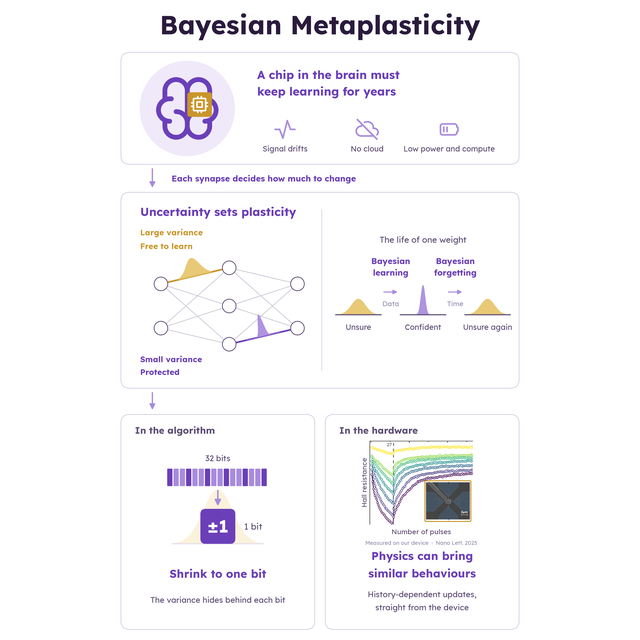
Figure 1. Bayesian metaplasticity, from the problem to the device. A chip implanted in the brain must keep learning for years without the cloud and with almost no memory or energy, so each synapse has to decide by itself how much to change. The thesis lets a weight's uncertainty set its plasticity: a large variance (gold) leaves the weight free to learn, a small variance (purple) protects it, data narrows the distribution (Bayesian learning) and time widens it back (Bayesian forgetting). The principle is brought onto the chip in two ways: in the algorithm, weights shrink to one bit while their variance survives as a hidden confidence; in the hardware, a magneto-ionic memory cell shows history-dependent updates of its own.
Jury members:
(en anglais) Crystallographic alignment and electric field control in bilayer graphene and boron nitride heterostructures
Centre de nanosciences et de nanotechnologies, , Palaiseau
Soutenance de thèse
Two-dimensional materials can be stacked into van der Waals heterostructures, exhibiting novel properties tunable through layer combination, interlayer spacing and crystallographic alignment. This thesis experimentally investigates the effects of moiré superlattice and perpendicular electric field on the electronic properties of heterostructures based on Bernal bilayer graphene (BBG) and hexagonal boron nitride (BN). Using dynamically rotatable devices, we tune the relative angle between graphene and the top BN layer via AFM tip driven rotation. Dual gated rotatable devices, developed during the thesis, allow to independently tune carrier density and displacement field while retaining angular control.
Charge transport measurements in local and non-local configurations, from low to high temperatures, reveal distinct electronic properties at 0° and 60° alignments of BBG and BN. Numerical simulations attribute these differences to distinct in-plane atomic relaxation at the two alignments, arising from inequivalent stacking configurations. Using dual gated devices, we disentangle the respective impact of moiré superlattice and displacement field in opening an energy gap at the charge neutrality point of BBG, revealing a non-trivial angular dependence of the built-in crystal field, in agreement with simulations. We further observe the anomalous gating effect in BN/BBG/BN heterostructures, marked by gate-induced hysteresis and gate ineffectiveness, and we identify the 30° ± 15° rotation between the two BN layers as the triggering parameter. We show that this effect can be switched ON and OFF by rotating the top BN layer, with angle control shifting the device between three distinct metastable states.
Together, these results show that the twist angle affects the properties of van der Waals heterostructures not only through the alignment of the main active layers, but through the angular configuration of all layers involved.
Jury members :
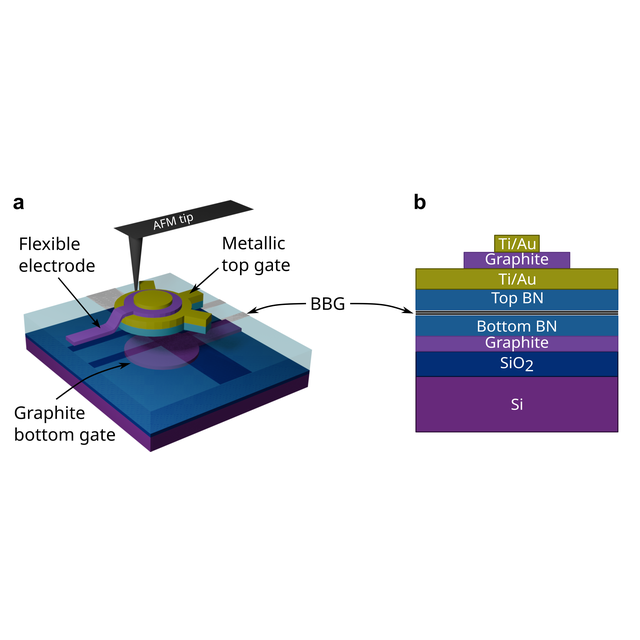
Figure 1. (a) and (b), Schematics of a dual gated rotatable device and its cross section. The device is composed of: Si/SiO2 substrate, graphite bottom gate, bottom BN flake, BBG Hall bar, top gate made of BN/Ti/Au rotator and flexible graphite electrode.
(en anglais) Active and passive devices on III-V platform for mid-IR integrated photonics
Centre de nanosciences et de nanotechnologies, , Palaiseau
Soutenance de thèse
The mid-infrared (2–20 𝜇𝑚) is of great interest for spectroscopy and optical communications, thanks to its characteristic molecular absorptions and its two atmospheric transparency windows (3–5 𝜇𝑚 and 8–12 𝜇𝑚). Advances in materials and epitaxial growth are driving the development of mid-IR photonic integrated circuits (PICs), offering the prospect to realize compact, robust, and energy-efficient systems for portable spectroscopy and real-time detection applications. The research on mid-IR PICs focuses on reducing propagation losses of dielectric waveguides. In addition, efforts are devoted to develop high-𝑄 resonators, versatile passive devices useful for filtering, wavelength division multiplexing and Kerr frequency comb generation (as demonstrated in the near infrared region). Furthermore, efficient and ultrafast integrated mid-IR modulators need developments, especially in the long-wave infrared region. They allow for an improved functionality of photonic integrated circuits, enabling electro-optic comb generation, synchronous detection, and high-speed data transmission for optical communications. The choice of a PIC platform depends heavily on the transparency of its constituent materials: III–V semiconductors are particularly attractive due to their low optical losses and their ability to monolithically integrate active and passive components. In this context, we investigated the performance of III–V passive devices, notably low-loss waveguides and high-Q resonators. In addition, we fabricated ultrafast amplitude modulators operating in the 8–12 μm band, which exploit intersubband transitions in asymmetric coupled quantum wells to achieve modulation.
Jury members:
Développement de texturation de surface pour la croissance épitaxiale latérale de III-V/Si
Centre de nanosciences et de nanotechnologies, , Palaiseau
Soutenance de thèse
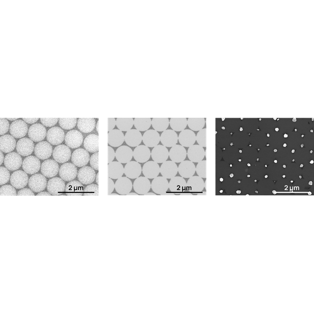
Cette thèse porte sur la texturation de surface du silicium en vue de l’intégration localisée de GaAs sur silicium par la méthode de croissance ELTOn (Epitaxial Lateral Overgrowth on Tunnel Oxide from nano-seeds), qui vise à obtenir une épitaxie sans défaut tout en maintenant un couplage électrique à travers un oxyde tunnel ultrafin. Les travaux abordent trois verrous technologiques majeurs : le contrôle du dopage résiduel du GaAs, le développement de procédés de lithographie à faible coût et à grande surface pour la croissance localisée, et l’ouverture localisée d’oxydes tunnel ultrafins. L’ensemble de ces études participe au développement futur d’architectures photovoltaïques tandem GaAs/Si à haut rendement.
Membres du jury :
Figures : De gauche à droite : (i) monocouche de nanobilles de polystyrène en réseau hexagonal sur Si, (ii) dépôt de 3 nm de Ge dans les interstices, (iii) après recuit, croissance localisée de GaAs sur Si.