PhD defense
Electric-field-assisted phase switching in semiconducting nanowires Contrôle par champ électrique de la structure cristalline de nanofils semi-conducteurs
Centre de nanosciences et de nanotechnologies, , Palaiseau
PhD defense
Polytypism, namely the existence of different stacking sequences of the crystal planes of the same material, provides a route to heterostructure formation in semiconductor nanowires. In III–V nanowires, such crystal phase heterostructures can be obtained through the controlled stacking of the cubic (zinc blende) and hexagonal (wurtzite) structures. One may thus form crystal phase quantum dots (CPQDs), which are promising building blocks for quantum devices.
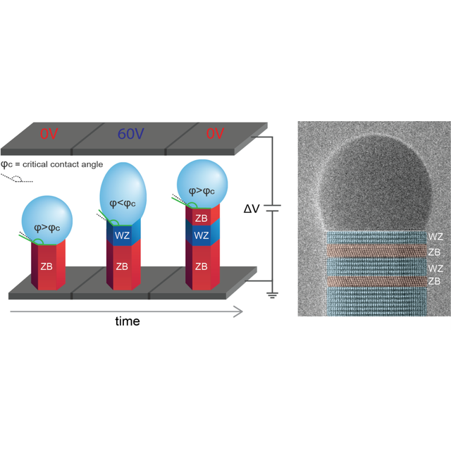
This thesis investigates the precise control of crystal phases in GaAs nanowires for CPQD fabrication using electric-field (E-field) assisted phase switching. Growth is performed by metalorganic chemical vapor deposition in the in situ NanoMAX transmission electron microscope, using specially designed cantilevers that provide a heated substrate and allow one to apply the E-field. The nanowires grow epitaxially in the vapor-liquid-solid mode with a liquid catalyst droplet at their tips. The method consists in changing quasi-instantaneously the shape of the droplet, and therefore its contact angle, by applying the E-field.
A major contribution is the demonstration of reversible crystal phase switching with atomically abrupt interfaces. Crystal phase insertion sizes down to a single monolayer are achieved. Several factors influencing CPQD formation are investigated. In addition to the droplet contact angle, a high enough temperature is found to be another key parameter for wurtzite growth. This is attributed to the temperature-dependent decomposition of metalorganic precursors, which may modify the surface energies of the nanowire facets and consequently affect crystal phase selection. In addition, the polarity of the E-field is found to affect the growth rate. Upon E-field reversal, growth rates become lower or higher than under no E-field. The possible causes of this effect are discussed.
Numerical simulations are used to investigate the effect of the E-field on the geometry of the droplet and to elucidate the mechanism of E-field-induced phase switching. The critical contact angle for phase selection is calculated from a combination of simulations and classical nucleation theory, and is compared with the experiments.
Jury members :
Rapporteure/rapporteur:
Examinateur/examinatrice:
Figure: By applying an electric field (E-field) during the growth of GaAs nanowires, we achieve reversible crystal phase switching between zinc blende (ZB) and wurtzite (WZ). The E-field dynamically deforms the catalyst droplet, reducing its contact angle j below the critical value for WZ formation and thereby triggering the ZB-to-WZ transition with monolayer precision. The TEM image shows a sharp crystal phase heterostructure obtained by this method, with WZ segments formed under E-field.

Métaplasticité Bayésienne : l’Incertitude comme Principe Algorithmique pour l’Apprentissage Embarqué
Centre de nanosciences et de nanotechnologies, , Palaiseau
PhD defense
Artificial intelligence is increasingly moving from data centers to edge devices, where neural networks must operate and learn continuously under severe constraints on memory, computation, and energy. At the same time, real-world environments are dynamic, requiring models to adapt to new information without overwriting what they have already learned. This thesis investigates a fundamental question for edge AI: can a neural network regulate its own plasticity and determine which information should be learned, retained, or forgotten?
The thesis explores Bayesian metaplasticity as a general framework for addressing this challenge. It first introduces MESU, a Bayesian approach to continual learning in which each network parameter maintains an estimate of its uncertainty. By incorporating uncertainty into the learning dynamics and retaining a bounded memory of past information, MESU allows parameters to adapt their plasticity according to their confidence. This provides a principled balance between stability and adaptation without requiring explicit task boundaries or replay buffers.
The thesis then introduces BiMU, a binary Bayesian extension designed for resource-constrained computing. By combining one-bit parameters with uncertainty-driven plasticity, BiMU reduces the memory and computational requirements of continual learning while preserving uncertainty over long, non-stationary data streams. This uncertainty can also be exploited to identify the most informative samples and enable selective adaptation through active learning, further improving the efficiency of learning at the edge.
Finally, the thesis investigates how the same principle can be implemented at the hardware level through magneto-ionic synapses. The intrinsic electrochemical dynamics of these devices introduce history dependence and nonlinear update dynamics, providing a potential physical substrate for metaplasticity in which the synapse itself regulates the magnitude of its updates according to its internal state and history.
Overall, this thesis connects Bayesian inference, continual learning, low-precision neural networks, and neuromorphic hardware around a common principle: uncertainty can act as a mechanism for regulating plasticity. This perspective points toward edge AI systems whose synapses can autonomously determine when and how strongly they should adapt to their environment, enabling continuous and energy-efficient learning under severe hardware constraints.
Figure 1. Bayesian metaplasticity, from the problem to the device. A chip implanted in the brain must keep learning for years without the cloud and with almost no memory or energy, so each synapse has to decide by itself how much to change. The thesis lets a weight's uncertainty set its plasticity: a large variance (gold) leaves the weight free to learn, a small variance (purple) protects it, data narrows the distribution (Bayesian learning) and time widens it back (Bayesian forgetting). The principle is brought onto the chip in two ways: in the algorithm, weights shrink to one bit while their variance survives as a hidden confidence; in the hardware, a magneto-ionic memory cell shows history-dependent updates of its own.
Jury members:
Crystallographic alignment and electric field control in bilayer graphene and boron nitride heterostructures
Centre de nanosciences et de nanotechnologies, , Palaiseau
PhD defense
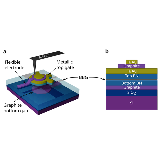
Two-dimensional materials can be stacked into van der Waals heterostructures, exhibiting novel properties tunable through layer combination, interlayer spacing and crystallographic alignment. This thesis experimentally investigates the effects of moiré superlattice and perpendicular electric field on the electronic properties of heterostructures based on Bernal bilayer graphene (BBG) and hexagonal boron nitride (BN). Using dynamically rotatable devices, we tune the relative angle between graphene and the top BN layer via AFM tip driven rotation. Dual gated rotatable devices, developed during the thesis, allow to independently tune carrier density and displacement field while retaining angular control.
Charge transport measurements in local and non-local configurations, from low to high temperatures, reveal distinct electronic properties at 0° and 60° alignments of BBG and BN. Numerical simulations attribute these differences to distinct in-plane atomic relaxation at the two alignments, arising from inequivalent stacking configurations. Using dual gated devices, we disentangle the respective impact of moiré superlattice and displacement field in opening an energy gap at the charge neutrality point of BBG, revealing a non-trivial angular dependence of the built-in crystal field, in agreement with simulations. We further observe the anomalous gating effect in BN/BBG/BN heterostructures, marked by gate-induced hysteresis and gate ineffectiveness, and we identify the 30° ± 15° rotation between the two BN layers as the triggering parameter. We show that this effect can be switched ON and OFF by rotating the top BN layer, with angle control shifting the device between three distinct metastable states.
Together, these results show that the twist angle affects the properties of van der Waals heterostructures not only through the alignment of the main active layers, but through the angular configuration of all layers involved.
Jury members :
Figure 1. (a) and (b), Schematics of a dual gated rotatable device and its cross section. The device is composed of: Si/SiO2 substrate, graphite bottom gate, bottom BN flake, BBG Hall bar, top gate made of BN/Ti/Au rotator and flexible graphite electrode.
Active and passive devices on III-V platform for mid-IR integrated photonics
Centre de nanosciences et de nanotechnologies, , Palaiseau
PhD defense
The mid-infrared (2–20 𝜇𝑚) is of great interest for spectroscopy and optical communications, thanks to its characteristic molecular absorptions and its two atmospheric transparency windows (3–5 𝜇𝑚 and 8–12 𝜇𝑚). Advances in materials and epitaxial growth are driving the development of mid-IR photonic integrated circuits (PICs), offering the prospect to realize compact, robust, and energy-efficient systems for portable spectroscopy and real-time detection applications. The research on mid-IR PICs focuses on reducing propagation losses of dielectric waveguides. In addition, efforts are devoted to develop high-𝑄 resonators, versatile passive devices useful for filtering, wavelength division multiplexing and Kerr frequency comb generation (as demonstrated in the near infrared region). Furthermore, efficient and ultrafast integrated mid-IR modulators need developments, especially in the long-wave infrared region. They allow for an improved functionality of photonic integrated circuits, enabling electro-optic comb generation, synchronous detection, and high-speed data transmission for optical communications. The choice of a PIC platform depends heavily on the transparency of its constituent materials: III–V semiconductors are particularly attractive due to their low optical losses and their ability to monolithically integrate active and passive components. In this context, we investigated the performance of III–V passive devices, notably low-loss waveguides and high-Q resonators. In addition, we fabricated ultrafast amplitude modulators operating in the 8–12 μm band, which exploit intersubband transitions in asymmetric coupled quantum wells to achieve modulation.
Jury members:
(in french)
Centre de nanosciences et de nanotechnologies, , Palaiseau
PhD defense
Emission and nonlinear optical properties in carbon nanotubes-on-silicon nanostructures
Centre de nanosciences et de nanotechnologies, , Palaiseau
PhD defense
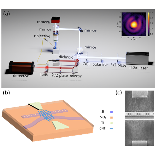
Thesis investigates the emission and nonlinear optical properties of single-walled carbon nanotubes (SWCNTs) integrated with silicon-based photonic nanostructures. The research focuses on the integration of carbon nanotubes with silicon photonics platforms to realize active and nonlinear optical functionalities for future integrated photonic systems. The thesis reviews the synthesis, deposition, optical characterization, and device-level integration of SWCNTs, with particular emphasis on photoluminescence enhancement and nonlinear optical effects.
Members of jury :
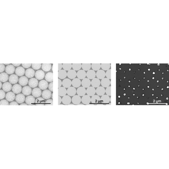
Figure 1. (a) Photoluminescence enhancement setup (b) Schematic of fabricated device (c) SEM image of dielectrophoresis deposited carbon nanotubes
Mid–infrared semiconductor saturable absorber mirrors (SESAMs) based on intersubband polaritons
, , Palaiseau
PhD defense
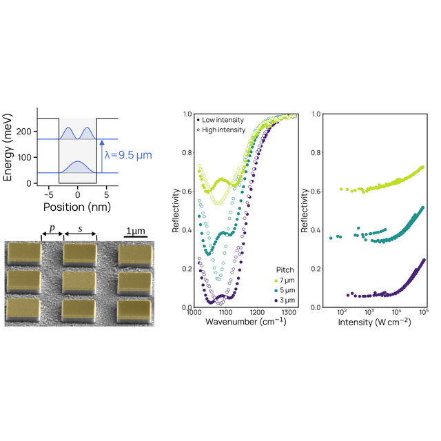
Ultrafast lasers revolutionized photonics by providing high peak intensities and pulse durations in the picosecond to femtosecond ranges. Passive mode-locking is the leading technique for generating short pulses, relying on saturable absorbers—nonlinear optical elements with intensity-dependent absorption. While semiconductor saturable absorber mirrors (SESAMs) are well-established for visible and near-infrared frequencies, a compact mid-infrared equivalent is lacking at longer wavelengths (λ > 3 µm). This thesis work proposes a novel mid-infrared SESAM concept based on the strong light-matter coupling between intersubband transitions in III-V semiconductor quantum wells and the resonant mode of metal-metal microcavities. Leveraging the strong field confinement in these structures, the saturation intensity of the intersubband transition is lowered to 10–20 kW cm−2, a level accessible by quantum (or interband) cascade lasers. We implemented a predictive tool based on coupled-mode theory to design the main figures-of-merit of a SESAM, such as modulation depth, non-saturable losses, low-intensity reflectivity and saturation intensity, exploiting both the sample geometry and the active region material. Time-domain pump–probe measurements revealed ultrafast decay times for these SESAMs of approximately 2 ps. These findings open the route towards applications with broad-gain laser sources such as mid-infrared fiber lasers, aiming to demonstrate self-starting passive mode-locking.
Members of jury :
Fig. The intersubband transition of a III-V semiconductor quantum well is embedded in an array of metal-metal microcavity resonators. The optical response of the sample is measured under low intensity - showing the appearance of intersubband polaritons in strong coupling - and high intensity - showing the absorption saturation of the intersubband transition. Pumping at the upper polariton frequency, the reflectivity of the device is measured varying the intensity of a quantum cascade laser. The result is the optical response of a semiconductor saturable absorber mirror (SESAM) tunable in the whole mid-infrared.

(in french)
C2N - Centre de Nanosciences et de Nanotechnologies, ,
PhD defense
(in french)
C2N - Centre de Nanosciences et de Nanotechnologies, Amphithéâtre,
PhD defense