Ajouter à son agenda
 Qiang YU
Soutenance de thèse
Polytypism, namely the existence of different stacking sequences of the crystal planes of the same material, provides a route to heterostructure formation in semiconductor nanowires. In III–V nanowires, such crystal phase heterostructures can be obtained through the controlled stacking of the cubic (zinc blende) and hexagonal (wurtzite) structures. One may thus form crystal phase quantum dots (CPQDs), which are promising building blocks for quantum devices.
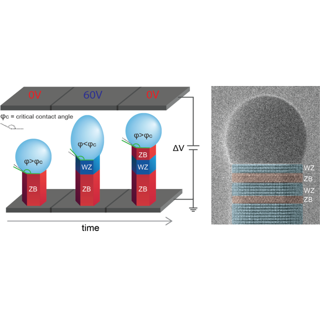
This thesis investigates the precise control of crystal phases in GaAs nanowires for CPQD fabrication using electric-field (E-field) assisted phase switching. Growth is performed by metalorganic chemical vapor deposition in the in situ NanoMAX transmission electron microscope, using specially designed cantilevers that provide a heated substrate and allow one to apply the E-field. The nanowires grow epitaxially in the vapor-liquid-solid mode with a liquid catalyst droplet at their tips. The method consists in changing quasi-instantaneously the shape of the droplet, and therefore its contact angle, by applying the E-field.
A major contribution is the demonstration of reversible crystal phase switching with atomically abrupt interfaces. Crystal phase insertion sizes down to a single monolayer are achieved. Several factors influencing CPQD formation are investigated. In addition to the droplet contact angle, a high enough temperature is found to be another key parameter for wurtzite growth. This is attributed to the temperature-dependent decomposition of metalorganic precursors, which may modify the surface energies of the nanowire facets and consequently affect crystal phase selection. In addition, the polarity of the E-field is found to affect the growth rate. Upon E-field reversal, growth rates become lower or higher than under no E-field. The possible causes of this effect are discussed.
Numerical simulations are used to investigate the effect of the E-field on the geometry of the droplet and to elucidate the mechanism of E-field-induced phase switching. The critical contact angle for phase selection is calculated from a combination of simulations and classical nucleation theory, and is compared with the experiments.
Jury members :
Rapporteure/rapporteur:
Examinateur/examinatrice:
Figure: By applying an electric field (E-field) during the growth of GaAs nanowires, we achieve reversible crystal phase switching between zinc blende (ZB) and wurtzite (WZ). The E-field dynamically deforms the catalyst droplet, reducing its contact angle j below the critical value for WZ formation and thereby triggering the ZB-to-WZ transition with monolayer precision. The TEM image shows a sharp crystal phase heterostructure obtained by this method, with WZ segments formed under E-field.
Amphithéâtre
Centre de nanosciences et de nanotechnologies
10 bld Thomas Gobert
91120 Palaiseau