







Results presented at the SPIE Nanophotonics XI conference (Proc. SPIE 14076, May 2026)
Silicon nitride (SiN) has established itself as an important material platform for integrated photonics due to its compatibility with CMOS fabrication processes, facilitating large scale-manufacturing and integration with existing photonics and electronics platforms. Its wide transparency window, low linear loss, moderate Kerr nonlinearity, and absence of two-photon absorption in the near infrared make it especially well-suited for high-performance nonlinear devices. Fully exploiting the nonlinear potential of SiN in the near-infrared depends on the quality of the fabrication process as nonlinear optical interactions require high optical intensities and long effective interaction lengths. This imposes strong requirements on waveguide loss, geometry, and material uniformity. Fabrication imperfections such as sidewall roughness, thickness variations, and residual stress can introduce scattering losses, degrade optical confinement, and alter dispersion profiles, thereby reducing nonlinear efficiency and limiting device performance. Furthermore, many nonlinear applications rely on precise dispersion engineering, often requiring thick, crack-free SiN films to achieve anomalous group-velocity dispersion. Consequently, the development of reliable, ultra-low-loss, and reproducible fabrication processes is a key step for advancing silicon nitride-based integrated nonlinear photonic devices and for translating these technologies into practical, scalable systems. The damascene process [1] was precisely established as the key fabrication strategy to realize ultra-low-loss SiN photonic devices. In this process, trenches corresponding to the desired device geometry are first patterned via lithography and anisotropic etching on the substrate layer. SiN is then deposited conformally, commonly using low-pressure chemical vapor deposition (LPCVD) to fill the preformed trenches. Excess material is subsequently removed by chemical mechanical planarization (CMP), leaving the SiN embedded only within the patterned regions. Finally, additional silicon dioxide cladding is deposited on top of the devices. Despite its advantages in enabling ultra-low-loss devices, the damascene process also presents several fabrication challenges and poses limitations that limit the use of this method for extended photonic devices. On key challenge lies in the CMP process, as this removal step is difficult to control uniformly across different feature sizes and pattern densities, requiring to use filler features to achieve high uniformity, and avoid defects such as dishing or erosion. Moreover, the resulting buried waveguide geometry can impose important limitations for other applications such as sensing and hybrid integration. As the SiN core is fully embedded within silicon dioxide, it restricts direct access to the optical mode. An alternative approach for fabricating SiN devices is the conventional subtractive process, which patterns the material directly through etching rather than embedding it via damascene fabrication. Although this process is more standard in commercial semiconductor foundries, several challenges must still be overcome to optimize it. For instance, the use of negative dispersion waveguides requires the use of thick SiN layers, which poses significant challenges due to the accumulation of intrinsic stress during deposition in LPCVD technique. Other challenges are the sidewall roughness introduced primarily through lithography imperfections and plasma etching processes and the absorption by the material impurities and hydrogen or oxygen-related bonds introducing absorption optical losses.
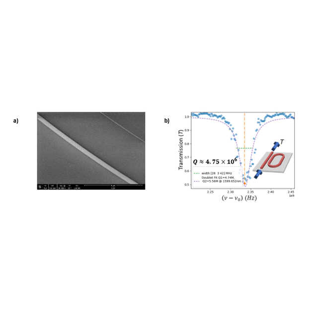
To overcome these limitations, a fabrication process was proposed. It was developed for an air-cladded 700nm silicon nitride platform, deposited using the LPCVD technique, over 3μm box of thermal silica, over a silicon substrate. Deep etching of the SiN layer was performed to define the chip boundaries and enable the separation of the wafer into individual samples. This was done to avoid cracking of the material when separating the individual dies. The resist used in this process was ZEP520A. The e-beam lithography process was performed using a multipass scheme, which averages real-time beam fluctuations during the patterning. The etching process was done using a fluorine-based reactive ion etching using CHF3 as the main gas that generates reactive fluorine radicals that chemically etch SiN and contributes to the passivation of the sidewalls. Ar was used to enhance physical sputtering and smooth the sidewalls, and N2 used to fine tune the passivation layer during the etching process. A final annealing process was performed to eliminate the N-H bonds left in the deposited material giving rise to well defined waveguides (Fig. 1 a)).
Optical losses were then measured using optical ring resonators by fine tuning the wavelength of a laser cavity and measuring the transmission spectra using an infrared photodetector [2]. Quality factors in the order of 5 million for multimode waveguides and 2 million for single mode ones were obtained (Fig. 1 b)). Devices exhibiting these levels of propagation loss and quality factors are well suited for applications in nonlinear optics, where strong optical confinement and manageable cavity lifetimes can still enable efficient frequency conversion or parametric processes [3]. These devices are also envisioned to be used in hybrid integration schemes with additional materials to increase the nonlinearities of the light interacting with them.
[1] M. H. P. Pfeiffer et al., Optica 5, 884-892 (2018)
[2] M. C. Diaz-Sanchez et al., Proc. SPIE 14076, Nanophotonics XI, 1407611 (26 May 2026), https://doi.org/10.1117/12.3099926
[3] X. Ji et al., Optica, 4, 6 (2017)
Maria Camila Diaz-Sanchez1, Yijun Yang1, Sebastian Alvarez-Ortega1, Etienne Herth1, David Bouville1 Daniele Melati1, Carlos Alonso-Ramos1, Delphine Marris-Morini1, Laurent Vivien1, Eric Cassan1
1Centre des Nanosciences et des Nanotechnologies, 91120 Palaiseau, France
Figure : Fig. 1: Optical characterization of SiN circuits: a) SEM view of a fabricated waveguide; b) Transmission of an all-pass ring resonator
Contact : Eric Cassan