







Multilayer photonic platforms enable large-scale photonic integrated circuits with compact, sophisticated routing and densely integrated components, but their fabrication requires the deposition of high-quality cladding layers and flat intermediate surfaces. Contact planarization using hydrogen silsesquioxane (HSQ) offers a low-cost solution, yet prior demonstrations have been limited to etch depths below 150 nm and minimum feature sizes of 100 nm, well short of the requirements of standard silicon photonic processes.
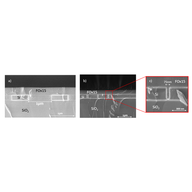
In this work, we present a bilayer HSQ deposition process that achieves effective planarization over a substantially broader dimensional range, covering trench widths from 75 nm to 1 μm and inter-structure spacings from 50 nm to 3 μm, for silicon etch depths of both 220 nm and 300 nm. Residual thickness variations of approximately 1 nm are obtained for narrow features with spacings between 50 nm and 500 nm, rising to approximately 7 nm for large 3 μm trenches. Inter-layer optical transitions between silicon and silicon nitride single-mode waveguides exhibit insertion losses as low as 0.3 dB per interface, confirming the optical quality of the planarized layers.
These results establish bilayer HSQ contact planarization as a practical, high-performance approach for silicon-silicon nitride multilayer photonic platforms.
References :
Optimization of hydrogen silsesquioxane planarization for multilayer photonic platforms
Micro and Nano Engineering, September 2026, Article: 100379, Volume 32
https://doi.org/10.1016/j.mne.2026.100379
Sarra Salhi, Jian Cao, Jean-Rene Coudevylle, François Maillard, Etienne Herth, Ali Madouri, Abdelmonaim Harouri, David Bouville, Xavier Lafosse, Teo Baptiste, Alan Durnez, Christophe Dupuis, Frédéric Mahut, Samson Edmond, Carlos Alonso Ramos, Laurent Vivien, Eric Cassan,
Daniele Melati
Centre de Nanosciences et de Nanotechnologies, Universite Paris-Saclay, CNRS, Palaiseau, 91120, France
Figure : Planarization results for the 220-nm SOI platform with flowable oxide (FOx). SEM images after the planarization process: (a) the widest trench (1 μm width), (b) the smallest trenches with (c) a zoom on the 75-nm-wide trench.
Contacts : Daniel Melati, Sarra Salhi