
Seminars
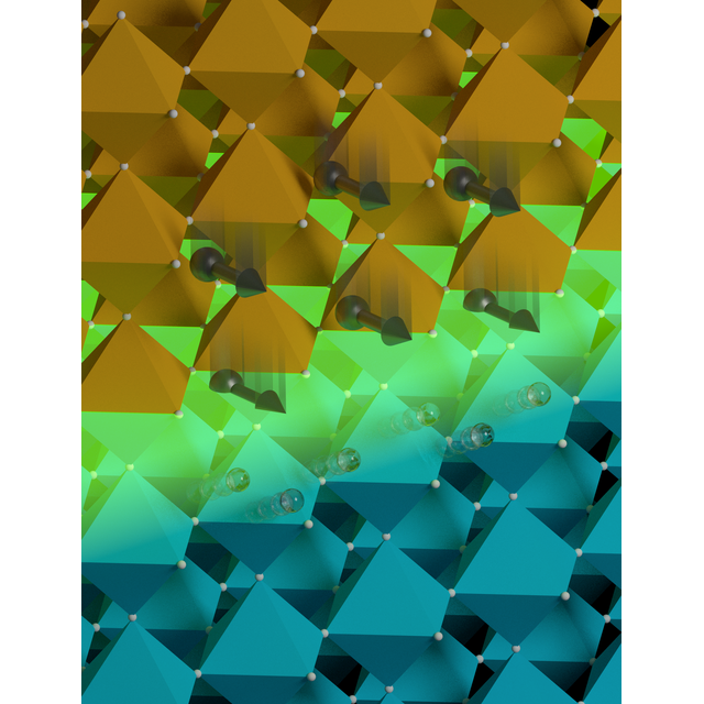
Magnetization dynamics in chiral spin textures
Centre de nanosciences et de nanotechnologies, Amphithéâtre, PalaiseauSeminars
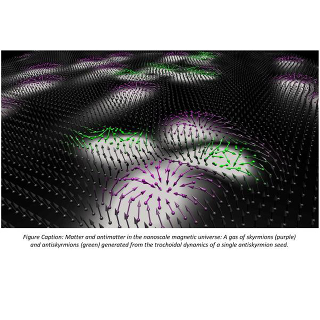
A variety of nontrivial spin textures can appear on the nanoscale as a result of competing magnetic interactions. A notable example being studied actively at present is the Dzyaloshinskii‐Moriya interaction (DMI), which results from spin-orbit coupling and chiral symmetry breaking in thin films and multilayers. The DMI not only confers a preferred handedness to spin configurations such as domain walls and skyrmions, but it also influences how excitations like spin waves propagate within a material.
I will describe some recent theoretical work on how the DMI influences dynamical magnetization processes in ultrathin films. In particular, I will discuss how nonreciprocity and focusing effects can occur for spin waves in continuous films and within chiral domain walls. I will also present novel features involving skyrmion and antiskyrmion dynamics, where pair generation processes result in excess skyrmion charges. Such systems represent an interesting playground in which we can probe how matter/antimatter asymmetry arises between topological magnetic charges.
Joo-Von Kim is a CNRS research associate at the C2N. After completing his PhD in theoretical physics at the University of Western Australia in 2002, he pursued a postdoctoral researcher position at the Institut d'Electronique Fondamentale before securing a tenured position in same laboratory in 2004. His research interests include nanomagnetism, spintronics, nonlinear dynamics, and stochastic processes, with a particular focus on how magnetization dynamics can be useful for information technologies.
Link: https://us02web.zoom.us/j/81600457076
On-chip micro/nanorobotic swimmers toward biomedical applications
Laboratory for Integrated Micro-Mechatronic Systems, En ligne,Seminars
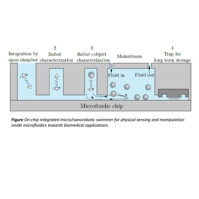
Untethered micro/nanorobotic swimmers are promising tool towards biologic or biomedical applications thanks to their highly accessible feature to tiny capillaries. However great challenges in design, fabrication and low Reynolds number physics have limited such applications. We integrated multidisciplinary technologies of micro/nanofabrication, microfluidics and microrobotics to those challenges. We recently developed highly energy efficient and fully controllable on-chip magnetic micro/nanorobotic swimmers with remote controlled functions such as cargo transport and sensing. A brief introduction to international joint laboratory (LIMMS-CNRS) at The University of Tokyo where I am currently hosted will be given at the beginning of seminar. Then I will introduce our recently developed micro and nanorobotic swimmers which can serve as mobile micromanipulator or physical sensor inside microfluidic channels. The presentation will be concluded by discussing ongoing and future perspectives toward biomedical applications.
Gilgueng Hwang obtained M.Sc. and Ph.D of Electrical Engineering from The University of Tokyo. After spending 2 years at ETHZ, Zurich, Switzerland and 2 years of postdoc at Sorbonne University, he joined to LPN (currently C2N) as CNRS researcher in October 2010. He obtained physics HDR degree in 2018. He is currently with the LIMMS-CNRS in the University of Tokyo, Japan. He has been awarded 5 world champions in the IEEE International Mobile Microrobotics Challenges.
Link: https://zoom.us/j/94322769401
Generation and manipulation of quantum states of light with AlGaAs chips
Centre de nanosciences et de nanotechnologies, , PalaiseauSeminars
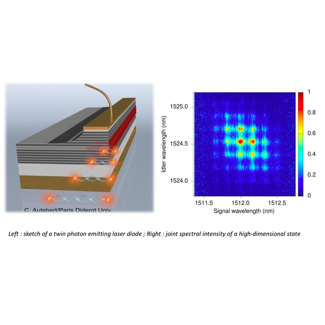
The development of miniaturized devices for the generation and manipulation of entangled states of light is one of the key issues on the way towards a broad diffusion of quantum information technologies. Different platforms are currently under study and, among them, semiconductors present a strong case for integrability; in this context, AlGaAs is particularly attractive to monolithically integrate active and passive components thanks to its compliance with electrical injection and to manipulate quantum photonic states via its large electro-optic effect. In this seminar, I will review our main results on the generation of quantum states of light with AlGaAs devices operating at room temperature and telecom wavelength and I will present our recent work on the generation and manipulation of high dimensional quantum frequency states of light opening promising perspectives for quantum simulations and computing.
Sara Ducci is professor at Université de Paris and member of the Laboratory « Matériaux et Phénomènes Quantiques ». She received her PhD in Physics at the University of Florence (Italy) in 2000, with a work on pattern formation in nonlinear optical systems. After a postdoctoral position at Laboratoire Kastler Brossel and a position as temporary assistant professor at Ecole Normale Supérieure de Cachan, she joined the University Paris Diderot in 2002. Her research focuses on the development of semiconductor sources of quantum states of light operating at room temperature and telecom wavelengths; the work ranges from device development to fundamental quantum optics and applications in quantum information. She has been awarded the Louis Ancel Prize of the French Physical Society in 2016 and she is honorary member of the Institut Universitaire de France.
Lien public: : https://us02web.zoom.us/j/84197969131
Please open the attached file below to access to the webinar link simply by clicking on it
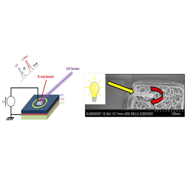
Photo-induced effects in ferroelectric thin film based devic
, Amphithéâtre, PalaiseauSeminars
Ferroelectric materials exhibit coupled degrees of freedom and possess a switchable electric polarization coupled to strain, making them good piezoelectrics and enabling numerous devices including non-volatile memories, actuators and sensors. Moreover, novel photovoltaic effects are encountered through the interplay of electric polarization with the materials optical properties. Consequently, the light-induced deformation in ferroelectrics, or photostriction, combining photovoltaic and converse piezoelectric effects, is under investigation in the quest for multifunctional materials.
Recent studies in ferroelectric thin films have reported photo-induced strain in the picosecond time range, thus opening a new route for ultrafast strain engineering and optical actuation in devices. However, the polarization is usually in as-grown state, so its contribution on the photostrictive response is not well understood.
In this presentation, we demonstrate that tuning the ferroelectric polarization allows controlling photo-induced current and ultrafast photo-induced strain in PZT thin films based capacitors. Recent promising results are also showing that light can be used to control the mechanical response of PZT MEMS. These measurements provide fundamental insight into light-matter interaction in ferroelectrics and exciting new avenues for materials functionality engineering.
Fig.: (Left) PZT ferroelectric capacitors measured by time-resolved X-ray diffraction, showing an in situ control of the fast photo-induced expansion or contraction following a UV pulse. (Right) PZT-based MEMS whose mechanical response can be tuned by light.
Il est possible d'accéder directement au séminaire via le lien présent dans l'annonce jointe
Lien public: https://zoom.us/j/95148164142
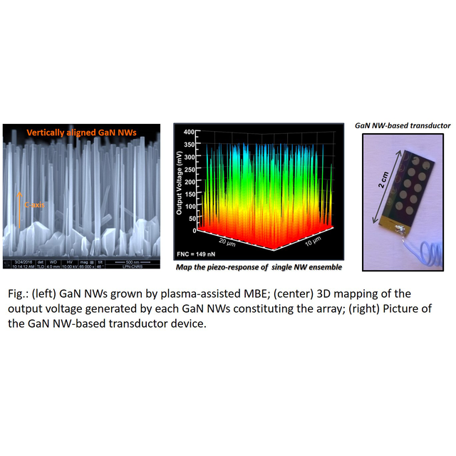
GaN Nanowires for Piezoelectric Generation
Centre de nanosciences et de naotechnologies, , PalaiseauSeminars
With the amount of connected objects constantly on a rise, it becomes critical to deal with the associated increase in energy consumption. Their energetic autonomy is today a key worldwide challenge, particularly for electronic systems operating in an environment with restricted, or even absent, electrical grid infrastructure. The miniaturization of the micro-devices for sensing and monitoring results in the reduction of their energy consumption, then opening perspectives for developing new autonomous intelligent systems.
Energy harvesting appears as a promising approach to power wireless micro-devices. Among renewable energies, the mechanical deformations and vibrations, harvested using piezoelectric materials, present the advantages to be ubiquitous and permanently available.
Recently GaN nanowires (NWs) have emerged as systems of interest for developing piezoelectric generators. Thanks to their superior mechanical properties, high sensitivity to applied force and exalted piezoelectric response over conventional 2D films and bulk materials, the NWs present undeniable advantages for significantly enhance the conversion efficiency of the generators.
In this presentation, we demonstrate the high potential of GaN NWs for piezo-generation. Our approach is based on systematic multiscale analyses going from the NW synthesis to the fabrication and testing of generators, passing through the characterization of the piezoelectric properties of unique NWs and the investigation of the piezo-mechanisms in play.
Bio: Dr. Noelle Gogneau received her PhD degree in physics in 2004 from the Grenoble Alpes University, France. After a post-doctoral position at EPFL, Switzerland, she joined the Laboratory for Photonic and Nanostructures (today the C2N) as CNRS researcher in 2006. From 2011, her research activities are centered on the growth of III-N NWs by PA-MBE and their characterization for Nano-Energy applications, with an emphasis on the piezoelectric properties of 1D-nanostructures for the development of a new generation of nano/piezo-generators.
Lien public: https://zoom.us/j/99637733548?pwd=NERpSkcxZVZ2Ui9lUEhvTG1LWXFIUT09
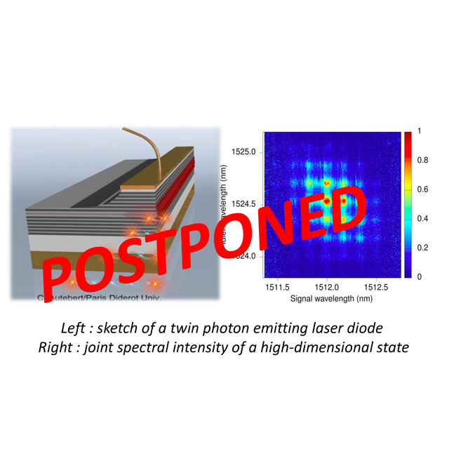
THE SEMINAR IS POSTPONED
Centre de Nanosciences et de Nanotechnologies, Amphithéâtre, PalaiseauSeminars
The seminar with Sara DUCCI is postponed to a later date.
Generation and manipulation of quantum states of light with AlGaAs chips
The development of miniaturized devices for the generation and manipulation of entangled states of light is one of the key issues on the way towards a broad diffusion of quantum information technologies. Different platforms are currently under study and, among them, semiconductors present a strong case for integrability; in this context, AlGaAs is particularly attractive to monolithically integrate active and passive components thanks to its compliance with electrical injection and to manipulate quantum photonic states via its large electro-optic effect. In this seminar, I will review our main results on the generation of quantum states of light with AlGaAs devices operating at room temperature and telecom wavelength and I will present our recent work on the generation and manipulation of high dimensional quantum frequency states of light opening promising perspectives for quantum simulations and computing.
Sara Ducci is professor at Université de Paris and member of the Laboratory « Matériaux et Phénomènes Quantiques ». She received her PhD in Physics at the University of Florence (Italy) in 2000, with a work on pattern formation in nonlinear optical systems. After a postdoctoral position at Laboratoire Kastler Brossel and a position as temporary assistant professor at Ecole Normale Supérieure de Cachan, she joined the University Paris Diderot in 2002. Her research focuses on the development of semiconductor sources of quantum states of light operating at room temperature and telecom wavelengths; the work ranges from device development to fundamental quantum optics and applications in quantum information. She has been awarded the Louis Ancel Prize of the French Physical Society in 2016 and she is honorary member of the Institut Universitaire de France.
External visitors should be register beforehand via e-mail at com@c2n.upsaclay.fr

THE COLLOQUIUM IS POSTPONED
Centre de Nanosciences et de Nanotechnologies, Amphithéâtre, PalaiseauSeminars
The Colloquium with Claudia Felser is postponed to a later date.
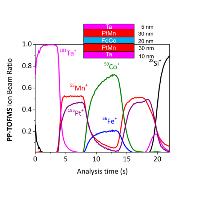
Ultra-Fast Compositional Depth Profile Analysis for Microelectronics Applications
Centre de Nanosciences et de Nanotechnologies, Amphithéâtre, PalaiseauSeminars
Abstract: Would you appreciate a tool capable of providing stoichiometry of freshly deposited thin films in just a few minutes?
In a context of growing competition, reducing the cycle time for materials is becoming crucial and requires rapid feedback for process optimization. For such fast feedback purposes, a plasma profiling time-of-flight mass spectrometry (PP-TOFMS) instrument (HORIBA Scientific, France) is now commercially available.
PP-TOFMS is a sputtering-based elemental depth profiling technique combining a pulsed radio-frequency argon plasma source (generating a glow discharge) for sample sputtering and ionization with an orthogonal time-of-flight mass spectrometer. PP-TOFMS produces, in a few minutes, nm-scale depth resolved profiles of all elements (including light ones) of the periodic table, over a wide dynamic range (from 100% down to ppm). A simple ratio of the number of ions detected from a given layer provides a calibration free semi-quantification.
Various data obtained with an instrument installed in the clean room of the CEA-LETI will be presented. We will illustrate how useful PP-TOFMS analysis turned out to be for materials designed for applications like power electronics (III-nitrides), phase change memories (GeSbTe) or magnetic sensors (FeCoB).
A comparison with ToF-SIMS will demonstrate the performance of PP-TOFMS in determining composition, detecting contamination, and measuring doping level.
Bio: Agnès Tempez is PP-TOFMS product manager since 2011 and an application scientist in the Nanoscopy AFM Raman team at HORIBA, France. She holds a Ph.D. in Analytical Chemistry from the University of Houston, Texas. She worked as a research scientist at Ionwerks Inc. (Houston) to develop time of flight mass spectrometry instrumentation for materials characterization and MALDI/ion mobility coupling for complex biological samples.
External visitors should be register beforehand via e-mail at com@c2n.upsaclay.fr
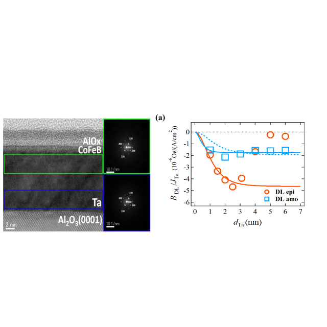
Epitaxially grown heavy metals towards efficient spin orbit torque and magnetization reversal
Centre de nanosciences et de nanotechnologies, Amphithéatre, PalaiseauSeminars
Spin current generation and magnetization reversal are core technologies to realize not only for a non-volatile memory but also for neuromorphic and probabilistic bit computing [1-3]. Spin-orbit interaction (SOI) becomes a key to efficiently generate spin current by spin Hall effect and an interface effect [4,5], and intensive studies have been conducted in various heavy metals (Pt, W and Ta). However, most studies are based on polycrystal or amorphous structures. High quality heterointerface would be necessary for precise control of spin-orbit-related phenomenon in a metal system.
We focus on epitaxial films for efficient control of spin current and magnetization [6-10]. We also focus on a heterointerface on polycrystal heavy metals as well as oxidation and nitridation of light metal Cu to realize large Rashba SOI [11-15]. We epitaxially grow Pt and a-Ta by employing sputtering method on MgO and Al2O3 substrates as shown in Fig. 1 for a-Ta case. We first reveal the spin relaxation mechanism by measuring magnetoconductance at cryogenic temperature. Induced weak antilocalization reveals that D’yakonov-Perel’ spin relaxation mechanism due to Rashba/ Dresselhaus SOIs is dominated in epitaxial Pt and Ta films [6-8]. This becomes contrast to polycrystal film where the impurity scattering governs the spin relaxation. We then investigated the spin-orbit torque and magnetization reversal with ferromagnetic layers [9,10,14,15]. Spin torque efficiency in a-Ta / CoFeB is enhanced from that of amorphous Ta (Fig. 2). Both epitaxial Pt and a-Ta enable the zero-field magnetization switching. I will also discuss about the spin current generation in W/Pt interface and Cu nitride structures for efficient spin orbit torque.
Prof. Makoto Kohda received his Master’s degree in engineering in 2002 and Ph.D degree in engineering in 2005 from Tohoku University, Sendai, Japan. After his PhD degree, he was an assistant professor (2005- 2010) and is an associate professor from 2010 at Department of Materials Science in Tohoku University. His current research interests are spin orbit interaction in semiconductor heterostructure and epitaxial metal films for efficient spin generation/manipulation and towards spin-orbitronics.
External visitors should be register beforehand via e-mail at com@c2n.upsaclay.fr
SrTiO3-based 2-dimensional electron gases for ultralow power spintronics
Centre de nanosciences et de nanotechnologies, Amphithéâtre, PalaiseauSeminars
One promising approach for beyond CMOS is the so-called MESO transistor proposed by Intel (for MagnetoElectric-Spin-Orbit), a spin-based non-volatile device in which magnetic information is written by a magnetoelectric element and read out by a spin-orbit element through the inverse spin Hall effect (ISHE) or the inverse Edelstein effect (IEE). The IEE occurs in systems with broken inversion symmetry such as two-dimensional electron gases (2DEG) displaying Rashba spin-orbit coupling and results in more efficient conversion than the ISHE.
In this talk, I will show that the 2DEG that forms at the interface of SrTiO3 (STO) with LaAlO3 or reactive metals such as Al may be exploited to interconvert spin and charge currents with very high efficiencies. By applying a gate voltage, we tune the position of the Fermi level in the complex multi-orbital structure of STO, which results in a strong variation of the conversion amplitude with sign changes. This can be related to the band structure through ARPES experiment and tight-binding calculations. Importantly, a finite spin to charge conversion effect persists at room temperature. In a second part, I will present gate-controlled, all-electrical spin current generation and detection in planar nanodevices free from ferromagnets and only based on a STO 2DEG.
Finally, I will propose a new approach to achieve a non-volatile control of spin-charge interconversion with Rashba 2DEGs based on ferroelectricity rather than ferromagnetism, that may pave the way to an entirely new family of ultralow power spintronics devices.
Manuel Bibes is a CNRS Research Director at the CNRS/Thales laboratory in Palaiseau, France. After a double PhD degree in France and Spain with a thesis on manganite interfaces (ICMAB Barcelona, 2001) he became a CNRS Researcher in 2003. Bibes has pioneered research lines on multiferroics, ferroelectric tunnel junctions and explored novel routes for the electrical control of magnetism and spin transport in oxide architectures. Bibes is the recipient of the 2013 EU40 Materials Prize of the E-MRS, the 2017 Descartes-Huygens prize, the 2017 Friedrich-Wilhelm Bessel award of the Humboldt Foundation and the laureate of two ERC grants.
Figure caption : Conversion of a spin current injected in the 2DEG at the LaAlO3/SrTiO3 interface into a charge current.
External visitors should be register beforehand via e-mail at com@c2n.upsaclay.fr