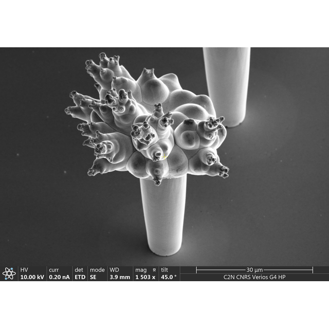
News

image not available

Measurement standards at the nanoscale for AFM and SEM microscopes

This article was published in the CNRS – La lettre Innovation (in French) in February 2019, under « Partenariats ». The Laboratoire National de métrologie et d’Essais and the Centre de Nanosciences et de Nanotechnologies1 co-developed …

Read more...
image not available

Linear electro-optic effect in a centrosymmetric semiconductor

Researchers from C2N demonstrated a high-speed Pockels effect in strained silicon waveguides, clearing the doubts raised over the last decade on its existence. The explosion of data demand imposed new requirements in terms of data transmission rate and …

Read more...
image not available

First laser effect observed in germanium direct bandgap

A collaboration of researchers from C2N and STMicroelectronics has obtained, for the first time, a laser effect with germanium as active material thanks to direct alignment of the electronic band diagram. Until now, this material was known to be …

Read more...
image not available

Coupled nano-oscillators capable of recognizing vowels according to a learning rule

Physicists have succeeded in fabricating a network of four coupled nano-oscillators capable of recognizing spoken vowels by tuning their frequencies according to an automatic rule of real-time learning. They show that high experimental recognition rates are a result of …

Read more...
image not available

Taming sound at the nanoscale

Physicists have proposed a new way to control the propagation of sound at the nanoscale. They put in evidence new ways of trapping sound at the interface between two chains of nano-resonators. Topology offers new degrees of freedom …

Read more...