Using angle-resolved photoemission spectroscopy (ARPES) combined with DFT calculations, physicists from the Center for Nanosciences and Nanotechnologies (C2N, Université Paris-Saclay / CNRS), in collaboration with researchers from Hunan University (China) demonstrated that high PL intensity value observed in WS0.4Se1.6 bilayers is due to the proximity of direct and indirect optical transitions.
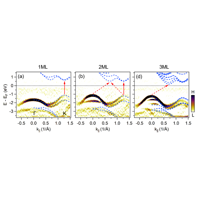
Transition metal dichalcogenides (TMDs) are usually characterized by a crossover from indirect to direct band gap semiconductor as the material thickness drops from several to a single monolayer. This transition can be followed optically as a large increase of the room temperature photoluminescence (PL) signal of at least one order of magnitude. Numerous studies on TMDs have revealed similar PL variation when these materials are reduced to a single layer. We demonstrate that this standard trend may show an exception for WS2(1−x) Se2x alloys. For a particular ternary alloy (x = 0.8), we observe a high PL intensity for monolayer and bilayer domains, for which the PL only decreases by a factor 2 compared to monolayer. To better understand this phenomenon, the electronic properties of WS2(1−x)Se2x (x = 0.8) have been studied using ARPES and density functional theory (DFT) calculations. Our results confirm the classic trend with a direct band gap for single ML alloys and indirect band gap for increasing number of layers. However the case of bilayer (x=0.8) is at the limit and presents both direct and indirect optical transitions. This robustness of PL intensity will ease material integration because it is more tolerant to thickness fluctuations.
The mat2D group at C2N (https://mat2d.c2n.universite-paris-saclay.fr) is expert in the electronic properties of 2D materials (Graphene, MX and MX2) Our activities focus on the design, manufacture and electronic properties of new hybrid heterostructures based on two-dimensional materials, toward the realization of a new generation of nanoelectronic devices. This publication is produced in collaboration with the Hunan University.
References
Indirect to direct band gap crossover in two-dimensional WS2(1−x)Se2x alloys
Cyrine Ernandes1, Lama Khalil1, Hela Almabrouk1, Debora Pierucci2, Biyuan Zheng3, José Avila4, Pavel Dudin4, Julien Chaste1, Fabrice Oehler1, Marco Pala1, Federico Bisti2, Thibault Brulé5, Emmanuel Lhuillier6, Anlian Pan3, and Abdelkarim Ouerghi1
npj 2D Materials and Applications 5, 7 (2021)
https://doi.org/10.1038/s41699-020-00187-9
Affiliations
1Université Paris-Saclay, CNRS, Centre de Nanosciences et de Nanotechnologies, 91120, Palaiseau,
2CELLS - ALBA Synchrotron Radiation Facility, Carrer de la Llum 2-26, 08290 Cerdanyola del Valles, Barcelona, Spain
3Key Laboratory for Micro-Nano Physics and Technology of Hunan Province, State Key Laboratory of Chemo/Biosensing and Chemometrics, and College of Materials Science and Engineering, Hunan University, Changsha, 410082 Hunan, China
4Synchrotron-SOLEIL, Université Paris-Saclay, Saint-Aubin, BP48, F91192 Gif sur Yvette, France
5HORIBA France SAS, Passage Jobin Yvon, Avenue de la Vauve, 91120 Palaiseau, France
6Sorbonne Université, CNRS, Institut des NanoSciences de Paris (INSP) F-75005 Paris, France
Figure: nano-ARPES second derivative spectra acquired on (a) 1 ML, (b) 2 ML, and (c) 3 ML WS2(1−x) Se2x (x = 0.8) along the Γ-K direction (photon energy 100eV). The associated DFT band calculations are shown as blue dashed lines.