News from Institut des sciences de l'ingénierie et des systèmes (INSIS) of CNRS - April 15, 2019 (released in French)
Thanks to its expertise in the realization of cryogenic high electron mobility transistors, a C2N team has enabled a Dutch team to observe at the atomic scale the mechanisms that explain the insulating nature of the surface of a cuprate, a metal-superconductor. The results were published in Nature Physics.
Some electronic phenomena in materials can only be observed at very low temperatures, close to absolute zero, in order to minimize thermal noise. For this purpose, researchers can use a low-temperature tunneling microscope (LT-STM), the tip of which operates at less than 4 Kelvin. However, observing certain electron behaviors of the material was still impossible, because of the existing electrical cable between the tip of LT-STM cooled at very low temperature and the amplifier at room temperature (300 Kelvin). Indeed, the capacity of this cable bypasses the signals when they exceed the kilo-hertz. In particular, this was a hurdle for researchers who wanted to study the mechanism by which a cuprate-type superconductor material may have an insulating surface.
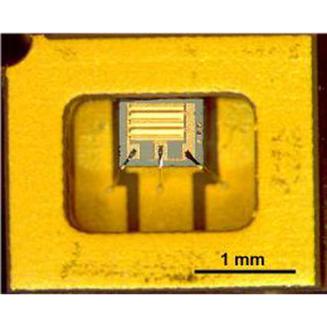
A team from the Centre for Nanoscience and Nanotechnology - C2N (CNRS / University Paris-Sud-University Paris-Saclay) has developed a solution using its expertise in the field of realization of cryogenic high electronic mobility transistors "cryoHEMTs". As part of a collaboration with physicists at Leiden University (the Netherlands), a MHz cryogenic amplifier has been optimized and located near the tip of an LT-STM operating at less than 4 Kelvin. Thanks to this device, the Dutch team was able to measure for the first time on the atomic scale the super-Poissonian noise - a characteristic signal of the electrons trapped around impurities - on the surface of the superconducting cuprate. This phenomenon explains the anisotropy of the superconductor, which is insulating in one direction.
The cryoHEMT, produced in the clean rooms of the C2N (one of the 5 Renatech network sites) is the fruit of years of research and development within the C2N. It illustrates the progress of the laboratory that masters the complete fabrication steps: materials, manufacturing processes (molecular beam epitaxy, electron beam lithography, ion beam etching ...), and the characterization of realized circuits. CryoHEMT opens a new horizon for LT-STM, but also for other areas of research at very low temperatures, such as mesoscopic physics, nanoresonators, detectors in astrophysics, or even dark matter detectors1.
1 For more information: http://phynano.c2n.universite-paris-saclay.fr/en/teams/nanofet/
Reference:
Charge trapping and super-Poissonian noise centres in a cuprate superconductor,
K. M. Bastiaans, D. Cho, T. Benschop, I. Battisti, Y. Huang, M. S. Golden, Q. Dong, Y. Jin, J. Zaanen & M. P. Allan.
Nature Physics (2018)
DOI: 10.1038/s41567-018-0300-z
Contact:
Yong Jin, CNRS Senior Researcher at C2N
Figure : CryoHEMT realized at C2N © Y. Jin/C2N