High-angle annular dark field (HAADF) images acquired in a scanning transmission electron microscope (STEM) contain a wealth information on the structure and chemical composition of semiconductor crystals down to the atomic level. To date, tapping into this information has required prohibitively computation-intensive simulations. A team at C2N now proposes an experimental approach to extract the same information faster and for larger viewing fields by combining HAADF-STEM and energy-dispersive X-ray spectroscopy.
In high-angle annular dark-field scanning transmission electron microscopy (HAADF-STEM), images are formed by collecting Rutherford-scattered electrons, hence encoding the chemical composition of the crystal under observation in the microscope in the contrast of the acquired image. Decoding this information requires a mean of externally calibrating the HAADF-STEM contrast. Until recently, such a quantification at the atomic scale has only been possible by comparing the experimental image to images derived from atomistic simulations. Such simulations are complex and can rapidly become prohibitively time-consuming when applied to images with large viewing fields.
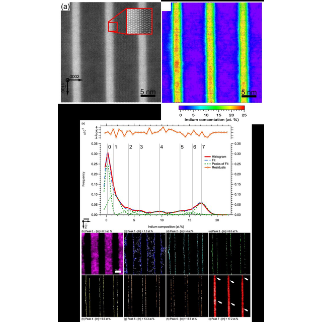
Researchers K. Pantzas and G. Patriarche recently developed an algorithm that relies on Energy-dispersive X-Ray spectroscopy (EDXS) as a substitute for simulations. This algorithm allows the user to straightforwardly compute atomically-resolved percent-wise precise compositional mappings of semiconductor alloys. In addition to compositional mappings, the algorithm also produces strain mappings from the HAADF-STEM image, giving the user a full picture of the structure of semiconductor crystals at the level of the single atomic column.
The team at C2N used the algorithm to study the interface between InGaN and GaN, the materials at the core of white light-emitting diodes. The team showed, for the first time, that the transition between the two materials occurs not continuously, but at discrete increments of composition. Beyond this applications, the capacity to measure strain and composition gives opens up new possibilities to study arbitrary quaternary alloys and semiconductor interfaces, such as those of the InAlGaAs superlattices, a system of paramount importance for the development of quantum cascade devices.
Reference
K. Pantzas and G. Patriarche
Ultramicroscopy, 220; 113152 (Jan 2021)
https://doi.org/10.1016/j.ultramic.2020.113152
Contact : Konstantinos Pantzas, CNRS Researcher, Materials Department
Affiliation
- Centre de Nanosciences et de Nanotechnologies – C2N (CNRS / Université Paris-Saclay)
Figure
(top) atomically resolved HAADF-STEM image (a) showing three InGaN wells in GaN barriers and (b) the corresponding mapping of the indium composition.
(bottom) Histogram of the indium compositions in the mapping and atomically resolved mappings of each of the distinct frequencies appearing in the histogram, revealing that the transition between GaN barriers and InGaN wells occurs through a succession of monolayers with distinct compositions.