Researchers at C2N and Thalès R&T develop a new material for integrated non-linear optics
Non-linear optics ihave yielded numerous applications in converting the wavelenght of laser light while preserving it’s other quantum properties. Interest is now growing in bring these applictations on photonic-integrated circtuits. Demonstrated compact nonlinear photonic circuits requires materials that demonstrate high conversion efficiencies, as a the length of the nonlinear crystal scales in inverse proportion to the square-root of efficiency. Achieving high efficiencies requires one to develop a meta-material that can be tailored to phase-match the frequencies of the waves involved in the nonlinear interaction.
A team at C2N lead by Konstantinos Pantzas recently developed one such material : Orientation-Patterned Gallium Phosphide (OP-GaP). Using a combination of metal-organic vapor-phase epitaxy (MOVPE), wafer bonding and e-beam lithography, the team created a meta-material consisting of domains of alternating 001 and 00-1 crystallographic orientations. Using this combination of techniques the dimensions of OP-GaP are well-defined to the level of individual atomic layers. Using this new OP-GaP platform, the team demonstrated conversion of telecom light to visible light, with a record efficiency of 200%/Wcm2
References
Continuous-Wave Second-Harmonic Generation in Orientation-Patterned Gallium Phosphide Waveguides at Telecom Wavelenghts
Konstantinos Pantzas1, Sylvain Combrié2, Myriam Bailly1,2, Raphaël Mandouze2, Francesco Rinaldo Talenti2,3, Abdelmounaim Harouri1, Bruno Gérard4, Grégoire Beaudoin1, Luc Le Gratiet1, Gilles Patriarche1, Alfredo De Rossi2, Yoan Léger5, Isabelle Sagnes1 & Arnaud Grisard2
ACS Photonics (2022)
DOI : https://doi.org/10.1021/acsphotonics.2c00156
Affiliations
1Centre for Nanosciences and Nanotechnology, CNRS, Université Paris-Saclay, UMR 9001, Palaiseau, France
2Thalès R&T, Palaiseau, France
3Dipartimento di Ingengeria dell’Informzione, Elettronica e Telecomunicazioni, Sapienza University of Rome, Rome, Italy
4III-V Lab, Palaiseau, France
5Institut Foton, CNRS, Université de Rennes, INSA, Rennes, France
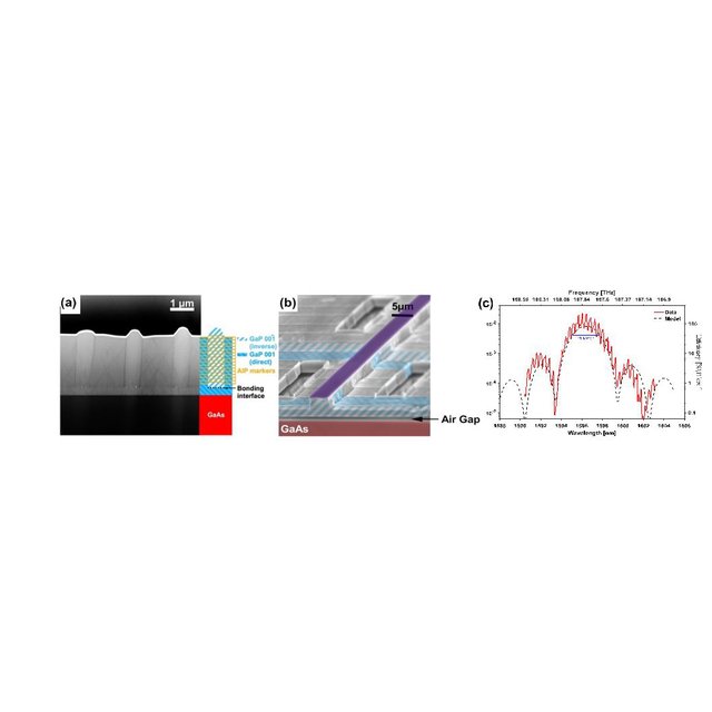
Figure : (a) HAADF-STEM micrograph of a cross-section of OP-GaP showing alternating domains of opposing crystallographic orientation (b) suspended air-clad OP-GaP shallow-ridge waveguide (c) efficiency curve of second-harmonic generation in OP-GaP showing a record efficiency of 200%/Wcm2
Contact C2N
Konstantinos PANTZAS