On-chip Brillouin optomechanics has great potential for applications in communications, sensing, and quantum technologies. Tight confinement of near-infrared photons and gigahertz phonons in integrated waveguides remains a key challenge to achieving strong on-chip Brillouin gain. Here, we propose a new strategy to harness Brillouin gain in silicon waveguides, based on the combination of genetic algorithm optimization and periodic subwavelength structuration to engineer photonic and phononic modes simultaneously. The proposed geometry is composed of a waveguide core and a lattice of anchoring arms with a subwavelength period requiring a single etch step. The waveguide geometry is optimized to maximize the Brillouin gain using a multi-physics genetic algorithm. Our simulation results predict a remarkable Brillouin gain exceeding 3300 W−1m−1, for a mechanical frequency near 15 GHz.
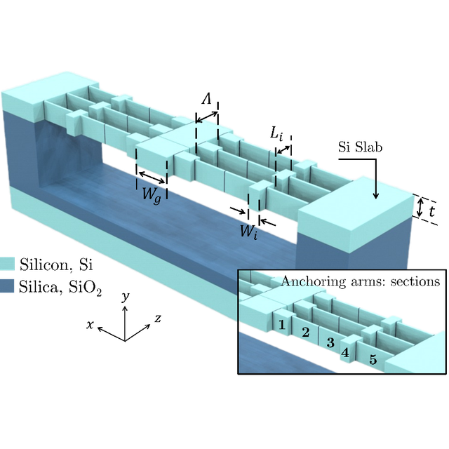
Brillouin scattering (BS) refers to the nonlinear interaction between optical and mechanical fields inside a material. In nanometric-scale silicon waveguides, BS is mediated not only by electrostrictive forces but also by strong radiation pressure on the boundaries of the structure. Efficient optomechanical coupling requires the simultaneous confinement of optical and mechanical modes, which is challenging in silicon-on-insulator (SOI) waveguides due to a strong phonon leakage toward the silica cladding. This limitation can be circumvented by isolating the silicon waveguide core removing the silica under-cladding. Forward Brillouin scattering (FBS) relies on longitudinally propagating photons and transversally propagating phonons. Hence, independent control of photonic and phononic modes is achieved by engineering the longitudinal and transversal subwavelength silicon membranes. Generally, previously reported structures require several etch steps of the silicon core to efficiently confine the mechanical mode, complicating the device’s fabrication. In this work, we propose a novel subwavelength-structured Si membrane requiring only one etch step of silicon. Our structure comprises a suspended central strip anchored to the lateral silicon slabs by a symmetric lattice of arms with a sub-wavelength longitudinal period. We develop an optimization method to design the waveguide geometry, combining multi-physics optical and mechanical simulations with a genetic algorithm (GA) capable of handling many parameters. The optimization process is done for an equivalent 2D geometry to reduce the computation resources. We use COMSOL Multiphysics software for the optomechanical simulations, considering transverse-electric (TE) polarized optical and in-plane mechanical modes. Based on the resulting optomechanical coupling calculations, GA optimization is used to find the optimum design of the anchoring lateral arms. Full 3D simulations are realized to verify the performance of the optimized geometry, and a Brillouin gain of 3310 W−1m−1 is obtained for a mechanical mode with a frequency of 14.579 GHz. The proposed structure exhibits a robust tolerance to fabrication imperfections such as under- and over-etching or stitching errors.
References
Genetic optimization of Brillouin scattering gain in subwavelength-structured silicon membrane waveguides
Paula Nuño Ruano, Jianhao Zhang, Daniele Melati, David González-Andrade, Xavier Le Roux, Eric Cassan, Delphine Marris-Morini, Laurent Vivien, Norberto Daniel Lanzillotti-Kimura, Carlos Alonso-Ramos
Optics & Laser Technology 161, p. 109130 (2023)
DOI: 10.1016/j.optlastec.2023.109130
Affiliation : Centre de Nanosciences et de Nanotechnologies, CNRS, Université Paris-Saclay, 10 boulevard Thomas Gobert, 91120, Palaiseau, France
Keywords : Brillouin scattering; Subwavelength; Genetic optimization
Contact : Carlos Alonso Ramos
Fig. 1. Proposed optomechanical waveguide. In the inset, the different sections of the anchoring arms are numbered from 1 to 5. The width of the waveguide core (w_g=400 nm), the period (Λ=300 nm), and the dimensions of the outermost section (L_5=50 nm, W_5=500 nm) remain fixed throughout the optimization process. The thickness of the silicon slab is t=220 nm.