Graphene, a single layer of carbon atoms tightly bound in a hexagonal honeycomb lattice to form a two-dimensional lattice, is a very interesting material with promising electronic, optical, chemical, and mechanical applicative potential [Geim and Novoselov, Nat. Mater. 6, 183 (2007)]. The properties of graphene make it suitable for a wide range of applications; however, its applicative future still depends on large scale technologies capable to robustly and reproducibly transfer its outstanding intrinsic properties into devices or complex structures. It must be recognized that a crucial technological problem, that still inhibits the applicability of high quality graphene material properties, is related to the patterning of this material using traditional top down instruments and lithographical methods. In this work, we will detail our investigations on applying a precise 30 keV Ga+ ion irradiation to selectively shape and modify a copper precursor surface for promoting the local growth of graphene surface domains. The morphology of these domains is investigated using scanning tunneling microscopy and spectroscopy to probe simultaneously the structural and the electronic properties at the atomic scale of the graphene films.
In this work we have demonstrated that single graphene domains can be fabricated, localized and organized directly via a specific Ga+ FIB patterning process. We have demonstrated that high FIB irradiation doses (106 ions/pixel) can resist the rearrangement process that occurs during the high temperature CVD preparation process, a temperature required in our experimental growth chamber to achieve high quality graphene films. The copper substrate annealing and copper native oxide removal performed around 1060°C induce a significant rearrangement of the copper precursor surface. Below the 105 ions/pixel threshold, the thin (around ten nm thick) FIB modified surface are erased by the annealing process. The line spacing, orientation or zigzag irradiation were found to provide identical results in the form of high quality localized 2D graphene films having sizes in coherence with the FIB irradiation pattern dimensions. The procedure we have presented relying on specific FIB irradiation can be carried as a batch process and hundreds of devices could be fabricated within a single patterning run.
Finally the investigated separation distances between two adjacent scanned lines ranging from 50 to 300nm representing a factor around 10 to 75 with respect to the calculated lateral projected ranges of 35 keV gallium ions (40nm), suggest that the sputtered and redeposited copper atoms (sputtering yield around 10) during the FIB irradiation process plays a central role in our approach.
This FIB assisted bottom-up growth technique we have presented would represent a major step towards a better control in the fabrication of structurally well-defined and well positioned 2D graphene flakes. Further work aiming at investigating the lower threshold ion dose required to initiate the growth of graphene is currently under investigation.
References
Selective growth of graphene films on gallium-focused ion beam irradiated domains Editor’s Pick
Jacques Gierak1, Gilles Raynaud1, Caroline Guiziou1, Jean René Coudevylle1, Ali Madouri1, Lars Bruchhaus2, Achim Nadzeyka2, Björn Whittman2, Ralf Jede2, Christophe David1, Jean Christophe Girard1
Journal of Vacuum Science & Technology B 40, 052602 (2022)
DOI : https://doi.org/10.1116/6.0002104
Affiliations
1 C2N, 10 Boulevard Thomas Gobert 91120 Palaiseau, France
2 Raith GmbH, Konrad-Adenauer-Allee 8, 44263 Dortmund, Germany
Contact : Jacques Gierak
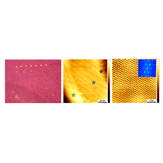
FIG. 1. (a) Optical microcopy image of the patterned structures after CVD growth of graphene. (b) Constant current STM topographic image (500nm x 500nm) obtained on a high dose FIB irradiation (106 ions/pixel) of the Cu(100). The Z colored scale varying from 0 to 20 nm is found to be identical to initial bare copper surface. (c) Higher resolution STM image (5nm x 5nm) performed on the same zone showing atomically resolved STM image of the surface graphene layer and its Fourier pattern in the inset. On this image the Z colored scale is varying from 0 to 130pm. The recorded shape of the individual carbon atoms is attributed to the anisotropic electronic structure of the tip apex atoms.