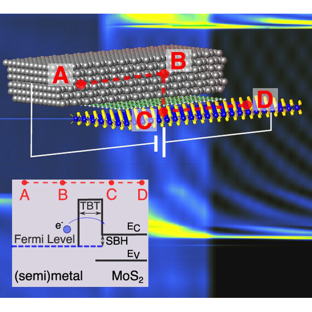
High contact resistance (RC) between 3D metallic conductors and single-layer 2D semiconductors poses major challenges toward their integration in nanoscale (opto)electronic devices. While in experiments the large RC values can be partly due to defects, ab initio simulations suggest that, even in defect-free structures, the interaction between metal and semiconductor orbitals can induce gap states that pin the Fermi level in the semiconductor band gap, increase the Schottky barrier height (SBH), and thus degrade the contact resistance. In this paper, we investigate, by using an in-house-developed ab initio transport methodology that combines density functional theory and nonequilibrium Green’s function (NEGF) transport calculations, the physical properties and electrical resistance of several options for n-type top metal contacts to monolayer MoS2, even in the presence of buffer layers, and for p-type contacts to monolayer WSe2. The delicate interplay between the SBH and tunneling barrier thickness (TBT) is quantitatively analyzed, confirming the excellent properties of the Bismuth-MoS2 system as an n-type ohmic contact. Moreover, simulation results supported by literature experiments suggest that the Au-WSe2 system is a promising candidate for p-type ohmic contacts. Finally, our analysis also reveals that a small modulation of a few angstroms of the distance between the (semi)metal and the transition-metal dichalcogenide (TMD) leads to large variations of RC. This could help to explain the scattering of RC values experimentally reported in the literature because different metal deposition techniques can result in small changes of the metal-to-TMD distance besides affecting the density of possible defects.
Ohmic Behavior in Metal Contacts to n/p-Type Transition-Metal Dichalcogenides : Schottky versus Tunneling Barrier Trade-off
1Daniel Lizzit, 1Pedram Khakbaz, 1Francesco Driussi, 2Marco Pala, and 1David Esseni
ACS Appl. Nano Mater. 6, 7, 5737–5746 (2023)
DOI: https://doi-org.ezproxy.universite-paris-saclay.fr/10.1021/acsanm.3c00166
1Polytechnic Department of Engineering and Architecture, University of Udine, Via delle Scienze 206, 33100 Udine, Italy
2Centre de Nanosciences et de Nanotechnologies - C2N (CNRS, Université Paris-Saclay) 91120 Palaiseau, France
Contact : Marco Pala