With the perspective of enhancing the physical properties of two-dimensional materials, the MAT2D team at C2N is studying the optical and electronic properties of 3R stacking tungsten diselenide (WSe2) grown on III-V semiconductor gallium phosphide (GaP). The used growth technique is molecular beam epitaxy, using a particular selenium passivation step of GaP substrate before the actual growth of WSe2. The research team and collaborators have clarified how the electronic properties of the 2D material are impacted by the underlying GaP substrate.
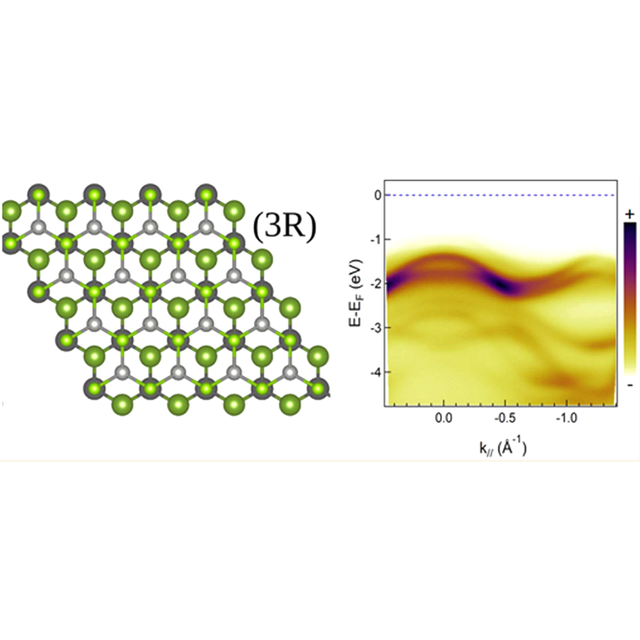
The growth of two-dimensional (2D) materials on conventional 3D semiconductors results in 2D/3D hybrid heterostructures, which offer a large variety of electronic properties depending on chemical composition, number of layers, and stacking order. Our team at C2N is studying the promising ferroelectric 3R phase of bilayer WSe2. After studying the electronic band structure of such 2D material in other form (Phys. Rev. B 108, 045417), we demonstrate that such rhombohedral-stacked bilayer of tungsten diselenide can be obtained by molecular beam epitaxy at the surface of a selenium-treated gallium phosphide substrate. We confirm the presence of a 3R-stacking bilayer using scanning transmission electron microscopy (STEM), micro-Raman spectroscopy, and high-resolution angle-resolved photoemission spectroscopy (ARPES). Our findings confirm the absence of chemical bonds at the interface, which confirms the quasi-van der Waals epitaxy of the 2D material on the III-V substrate. Our ARPES measurements reveal the expected valence band of WSe2 with the band maximum located at the Γ point of the Brillouin zone. The comparison with DFT calculations on free-standing bilayer WSe2 confirms the rhombohedral nature and the weak quasi-van der Waals interaction between the 2D material and the (selenium-treated) 3D substrate.
Reference :
Quasi van der Waals Epitaxy of Rhombohedral-Stacked Bilayer WSe2 on GaP(111) Heterostructure
Aymen Mahmoudi1, Meryem Bouaziz1, Niels Chapuis2, Geoffroy Kremer1, Julien Chaste1, Davide Romanin1, Marco Pala1, François Bertran3, Patrick Le Fèvre3, Iann C. Gerber4, Gilles Patriarche1, Fabrice Oehler1, Xavier Wallart2, Abdelkarim Ouerghi1
ACS Nano 2023, 17, 21, 21307–21316
DOI : https://doi.org/10.1021/acsnano.3c05818
Affiliations
1Université Paris-Saclay, CNRS, Centre de Nanosciences et de Nanotechnologies, 91120, Palaiseau, Paris, France
2Univ. Lille, CNRS, Centrale Lille, JUNIA ISEN, Univ. Polytechnique Hauts de France, UMR 8520-IEMN F59000 Lille France
3Synchrotron SOLEIL, L'Orme des Merisiers, Départementale 128, 91190 Saint-Aubin, France
4Université de Toulouse, INSA-CNRS-UPS, LPCNO, 135 Avenue de Rangueil, 31077 Toulouse, France
Contact : abdelkarim.ouerghi@c2n.upsaclay.fr
Figure : Schematic representation of the top view of 3R bilayer WSe2 stacking sequences and ARPES measurement of the valence band along the ΓK high-symmetry direction
Keywords : 2D materials - MBE - 2D on 3D heterostructure - electronic band structure - bilayer WSe2 - DFT