In recent years, several well-established 3D substrates have been considered for the van der Waals epitaxy of 2D-transition metal dichalcogenides, yet require a proper surface passivation treatment. In the framework of a collaboration between IEMN and C2N, the structural and electronic properties of well-ordered Se-terminated GaP(111)B surfaces by molecular beam epitaxy are studied. The key role of combining atomic hydrogen and cracked phosphine to prepare a smooth P-rich surface with a (2×2) reconstruction on n- and p-doped GaP(111)B is highlighted. The evolution of the surface electronic properties after exposure to a selenium flux is then investigated. The GaP(111)B surface exhibits a systematic change in reconstruction from a (2×2) to a (1×1) pattern, accompanied by a modification of the chemical environment mainly in the outermost P-terminated layer. The absence of GaSe layer formation is evidenced through photodiffraction experiments, while the band structure of the Se-passivated surface is shown to originate from that of GaP(111)B. An effective partial electronic passivation of the surface is further revealed by the evolution of the band bending and surface dipole measured with ultraviolet photoemission spectroscopy. This realization of a Se-terminated GaP(111)B substrate opens new perspectives for the development of 2D/3D heterostructures of strong interest for nanoelectronic and optoelectronic applications.
The development of heterostructures combining 2D materials - such as transition metal dichalcogenides (TMDs) - and 3D substrates is gaining increasing attention, as it enables the combination of the unique properties of monolayer materials with the robustness and integration potential of commercial substrates. However, it is necessary to prepare the 3D substrate beforehand so that its surface is perfectly deoxidized and compatible with so-called quasi–van der Waals epitaxy (i.e., minimally chemically bonded while still providing a high-quality interface). This study focuses on the preparation of the GaP(111)B surface, including a preliminary deoxidation step followed by selenium (Se) surface passivation, aimed at removing the substrate’s dangling bonds and thereby promoting TMD growth.
To this end, the GaP(111)B surface is first deoxidized in a III-V epitaxy chamber using a combination of atomic hydrogen and cracked phosphine at relatively low temperature. This process results in a well-defined (2×2) surface reconstruction, observed for both n- and p-doped substrates.
The surface is then transferred under ultra-high vacuum condition to a second epitaxy chamber dedicated to TMD growth, where it is exposed to a selenium flux at temperatures ranging from 450°C to 700°C. The surface reconstruction evolves from the previously observed (2×2) to a (1×1) pattern, suggesting that Se modifies the chemical environment of the outermost layer of the substrate. Structural analyses show that only the topmost phosphorus layer is modified, with no evidence of a complete GaSe layer formation.
In addition, angle-resolved photoemission spectroscopy (ARPES) measurements reveal that the dominant electronic band remains that of GaP, rather than that of a newly formed GaSe phase. Combined X-ray and UV photoelectron spectroscopy (XPS-UPS) measurements demonstrate changes in band bending and surface dipole, indicating effective partial passivation of surface states.
Finally, the study highlights that the passivation effect is strongly dependent on the Se flux. A high flux (3-5×10⁻⁶ Torr) leads to undesirable penetration of Se atoms into the top GaP layers, whereas a lower flux (3-5×-7 Torr) provides an optimal compromise between surface passivation and preservation of the GaP structure.
In conclusion, the study demonstrates that selenium passivation of GaP(111)B represents a promising approach to create a stable interface for the quasi–van der Waals epitaxial growth of TMDs. This surface preparation step is essential for the realization of next-generation 2D/3D heterostructures, with potential applications in nanoelectronics and optoelectronics.
Références
Electronic properties of the selenium passivated GaP(111)B surface : towards growth of large scale quasi-van der Waals 2D/3D heterostructure
Niels Chapuis1, Corentin Sthioul1, Aymen Mahmoudi2, Meryem Bouaziz2, Christophe Coinon1, Louis Thomas1, Davide Romanin2, Gilles Patriarche2, Fabrice Oehler2, Abdelkarim Ouerghi2 and Xavier Wallart1
Physical Review Material 9, 074002 (2025)
DOI : https://doi.org/10.1103/pv8b-89gg
Affiliations
1Université Lille, CNRS, Centrale Lille, Junia, Université Polytechnique Hauts-de-France, UMR 8520 – IEMN – Institut d’Electronique de Microélectronique et de Nanotechnologie, F-59000 Lille, France
2Université Paris-Saclay, CNRS, Centre de Nanosciences et de Nanotechnologies, 91120 Palaiseau, Paris, France
Mots-clefs : Van der Waals, 2D materials, Transition Metal Dichalcogenides, Electronic Structure, Photoemission
Contact : Niels Chapuis
This work is supported by Renatech through the C2N Nanotechnology Platform, as well as by the ANR Tunne2D and PEPR ADICT programs.
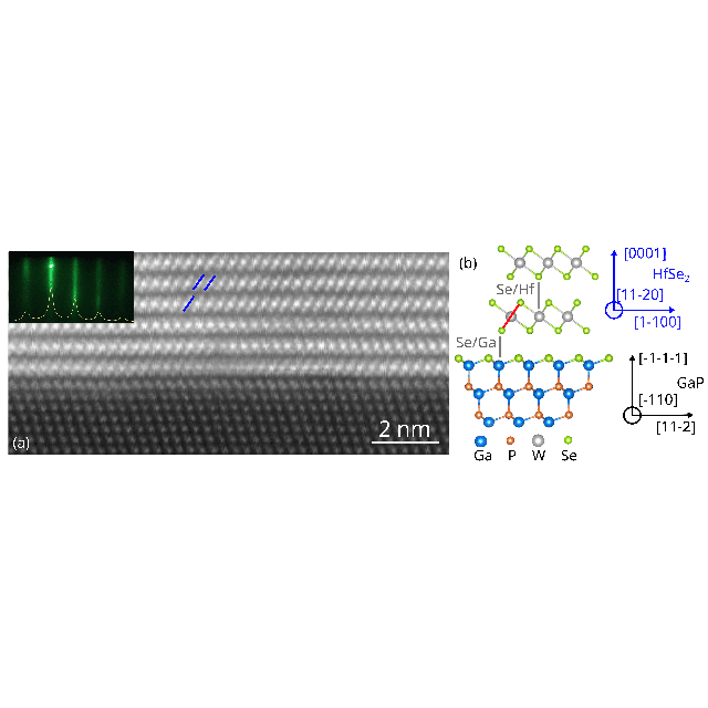
Figure : example of quasi van der Waals epitaxy on a Se-passivated GaP(111)B surface . (1×1) RHEED pattern and HAADF-STEM image of a HfSe2/Se-GaP(111)B heterostructure grown with MBE (a) and the associated side view schematic created with VESTA (b).