This article was published in the CNRS – La lettre Innovation (in French) in February 2019, under « Partenariats ».
The Laboratoire National de métrologie et d’Essais and the Centre de Nanosciences et de Nanotechnologies1 co-developed a nanoscale transfer standard prototype that calibrates atomic force and scanning electron microscopes. The standard is based on the meter of the International System of Units and thus provides an essential link for reliable dimensional measurements.
Nanotechnologies make it possible to provide materials with new mechanical, electrical or optical properties. For the many research and industrial laboratories active in this field it is necessary to correlate properties that appear only at the nanoscale with reliable dimensional measurements. It is therefore essential to link the measurements made at the nanometer scale with the definition of the meter in the International System of Units (SI).
To date, users of Atomic Force Microscopes (AFMs) and Scanning Electron Microscopes (SEMs), which measure the dimensions of nanostructures (surface roughness, thickness of thin layers, depth of nanometric patterns, etc.), have no standard to calibrate their instruments. Calibrations are done using periodic gratings of micrometric patterns, leading to high levels of uncertainty on the measurements made thereafter. To fill this gap the Laboratoire National de métrologie et d’Essais and the le Centre de Nanosciences et de Nanotechnologies1 have jointly developed a nanoscale measurement transfer standard2.
To realize a transfer standard, a reference measurement is first required. Several years ago the Laboratoire National de métrologie et d’Essais developed such a standard using an AFM. The position of the AFM tip relative to the sample is determined very precisely by laser interferometers whose wavelength is calibrated with respect to the frequency stabilized reference laser used for the definition of the meter. This ‘metrological’ AFM thus makes it possible to calibrate the dimensional characteristics of transfer standards (in particular structures having periodic patterns and controlled operating steps) with uncertainties in the order of nanometer (nm) .
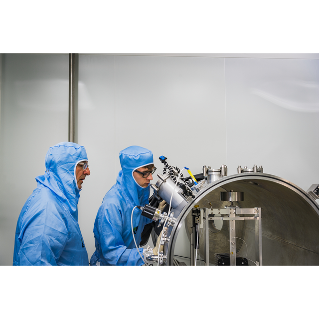
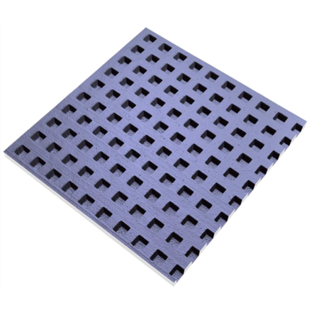
The Centre de Nanosciences et de Nanotechnologies have now implemented the nanofabrication technologies of the standard. This consists of a 2D periodic grating, etched on a 250 μm x 250 μm surface in the center of a 10 mm x 5 mm silicon substrate. The grating is first patterned by electron beam lithography (direct writing by an electron beam of a few nanometers in diameter) in a polymer, which serves as a mask during the transfer into silicon via dry etching. The nominal grating pitch is 900 nm (along the X and Y axes) and the nominal height 60 nm. The uncertainties amount to ± 2 nm for the grid pitch and ± 1 nm for the step height.
From this P900H603 transfer standard it is hence possible to extract an average value of the grating pitch, allowing a standard calibration of the instruments along the X and Y axes (AFM and SEM), and a value of the average step height for the Z-axis calibration (AFM). The determination of these characteristic dimensions by means of the LNE ‘metrological’ AFM will enable certified standard dimensions and their corresponding uncertainties (± 2 nm for the grid pitch and ± 1 nm for the step height).
1 C2N (CNRS/Université Paris-Sud)
2 A transfer standard makes it possible to link measurements made with the primary instrument (here the ‘metrological’ AFM) to a conventional laboratory instrument.
3 The development of this transfer standard is a continuation of the actions of the Club nanoMétrologie, created in 2011, which is the subject of a partnership agreement between LNE and the CNRS represented by UPS C'Nano. The club now has nearly 400 members, 30% of whom are industrial companies. Among its actions, the club leads several working groups around nanometrology, one of which focuses on the traceability of measurements at the nanoscale and in particular the definition of requirements for measurement standards of transfer and reference materials.
Contacts:
- Christian Ulysse / Deputy technical director of the Micro- and Nano-Technology Innovation Platform at C2N
- Luc le Gratiet / chargé de mission Partnership and Valorisation at C2N
- Georges Favre / LNE-Nanotech Director