
Seminars
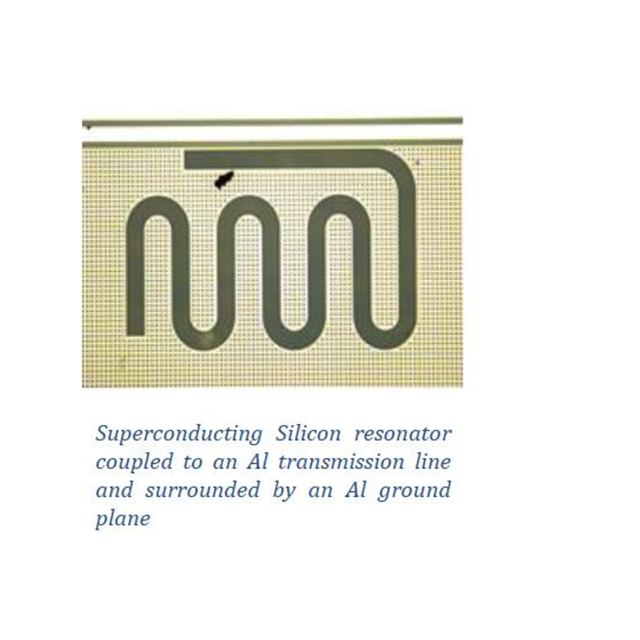
Strongly non-linear superconducting silicon resonators Francesca Chiodi
Centre de Nanosciences et de Nanotechnologies, Amphithéâtre, PalaiseauSeminars
Silicon is one of the most well-known materials, and the main actor in today electronics. Despite this, silicon superconductivity was only discovered in 2006 in laser doped Si:B samples. Laser annealing is instrumental to cross the superconductivity threshold, as the required doping is above the solubility limit, and cannot be reached using conventional micro-electronic techniques. Laser doping allows the realization of epitaxial, homogeneous, thin silicon layers (5-300 nm) with extreme active doping as high as 11 at. %, and without the formation of B aggregates. Silicon is a disordered superconductor, with a lower carrier density (1020 – 1021 cm-3) than metallic superconductors, a critical temperature modulable with doping from 0 to 0.7 K, and a relatively high resistivity that allows to easily match the devices to the void impedance.
After demonstrating all-silicon SQUIDs and Josephson junctions, we have realized microwave silicon resonators, working in the 1-10 GHz range and with quality factors about 4000. We have shown a strong non-linear response with power, observing a Kerr coefficient of the order of 300 Hz/photon where less than 1 Hz/photon was expected. This suggests that, once the losses sources identified and reduced, silicon resonators may be promising candidates for Kinetic Inductance Detectors. To better understand the losses and recombination mechanisms, we have measured the relaxation dynamics of the resonators following a light or a microwave pulse.
Francesca CHIODI is Maître de Conférences at Université Paris Sud. She joined the ‘Laser epitaxy’ group in 2011, to work on laser ultra-doping of Si and Ge, and to develop and investigate the first superconducting Si devices. She graduated from ENS, Paris, obtained a PhD at LPS, on the dynamics of long SNS Josephson junctions, and joined as a Post-Doc at Material Sciences Dept., Cambridge, UK, on triplet superconductivity in inhomogeneous SFS Josephson junctions.
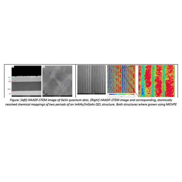
MetalOrganic Vapor Phase Epitaxy (MOVPE) for Photonics
Centre de Nanosciences et de Nanotechnologies, Amphithéâtre, PalaiseauSeminars
Organo-metallic chemical vapor epitaxy is a well-established technique used for the growth of highly complex heterostructures combining a variety of semiconductor alloys with a multitude of applications in photonics. Research in MOVPE at the C2N focuses at pushing the limits of what is feasible with this technique, tackling the growth of novel alloys such as (Si)GeSn, challenging due to their inherent immiscibility, and advanced heterostructures, such as quantum cascade devices, challenging to the complexity of their structure that consists of hundreds of layers that are only a few monolayers thick.
After a general introduction to the technique and an overview of the activity at the C2N, the seminar will delve more deeply in the subject of GeSn alloys and InAlAs/InGaAs quantum cascade structures, and showcase how one can achieve the required level of control over matter to produce novel photonic devices.
Konstantinos Pantzas is a researcher at the Centre de Nanosciences et de Nanotechnologies (C2N). His research evolves around the MOCVD growth of new materials and complex heterostructures for mid-infrared photonics. He received his predoctoral education at Supelec and holds a PhD in Material Science from the University of Lorraine in 2013 and a PhD in Electrical and Computer Engineering from the Georgia Institute of Technology in 2015. Prior to his appointment to the CNRS in 2016, he worked as was a post-doctoral research fellow at the Laboratoire de Photonique et de Nanostructures (ex-LPN, now C2N).
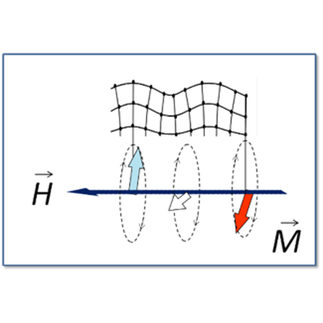
Ultrasonic drive of magnetization dynamics
Centre de Nanosciences et de Nanotechnologies, Amphithéatre, PalaiseauSeminars
Magnetostriction links the shape of a magnetic material to its magnetization direction. Kittel recognized early on the interest of applying this strain dynamically to induce magnetic resonance [1]. His ideas have seen a recent revival of interest when combined to a wide range of optical or electrical acoustic wave excitation techniques. These waves are widely used in the fields of semiconductors physics, nanophotonics, and quantum optomechanics. In the Gigahertz range, they become relevant to magnetism physics, as these are typically the eigenfrequencies of the magnetization in most ferromagnets. I will describe the work we have been doing on (Ga,Mn)As using sub-GHz surface acoustic waves (SAWs) to manipulate, control, and switch magnetization - even in the absence of any applied magnetic field [2,3,4]. I will detail the experimental technique we have developed that enables us a spatio-temporal detection of these ultrasound driven magnetization dynamics. I will conclude by some perspectives on the use of magneto-acoustics in both magnetic and acoustic devices.
[1] L. Thevenard et al., “Irreversible magnetization switching using surface acoustic waves,” Phys. Rev. B 87, 144402, 2013.
[2] L. Thevenard et al., “Precessional magnetization switching by a surface acoustic wave,” Phys. Rev. B 93, 134430, 2016.
[3] P. Kuszewski et al., “Resonant magneto-acoustic switching: influence of Rayleigh wave frequency and wavevector,” J. Phys. Condens. Matter 30, 244003, 2018.
[4] P. Kuszewski et al., “Optical probing of Rayleigh wave driven magneto-acoustic resonance,” Phys. Rev. Appl. 10, 034036, 2018.
Laura THEVENARD: She did her PhD on the dilute magnetic semiconductor GaMnAs at the Laboratoire de Photonique et Nanostructures with Aristide Lemaître on (Ga,Mn)As. She then went on to do a post-doc on Permalloy nanostructures in the group of Russel Cowburn, who was then located within Imperial College London. A few years after arriving at Institut of Nanosciences of Paris in 2009 (Sorbonne Universités campus) as a CNRS researcher, she developed with C. Gourdon, colleagues from the lab's Acoustics team, and A. Lemaître from the C2N, an original strategy to manipulate, control, and switch magnetization using surface acoustic waves of up to 1 GHz. The main experimental techniques are based on the magneto-optical kerr effect, that we implement either statically to perform magnetic domain imaging, or on a "pump-probe" set-up to access magnetization dynamics. In 2015 she received the Bronze Medal of the CNRS.
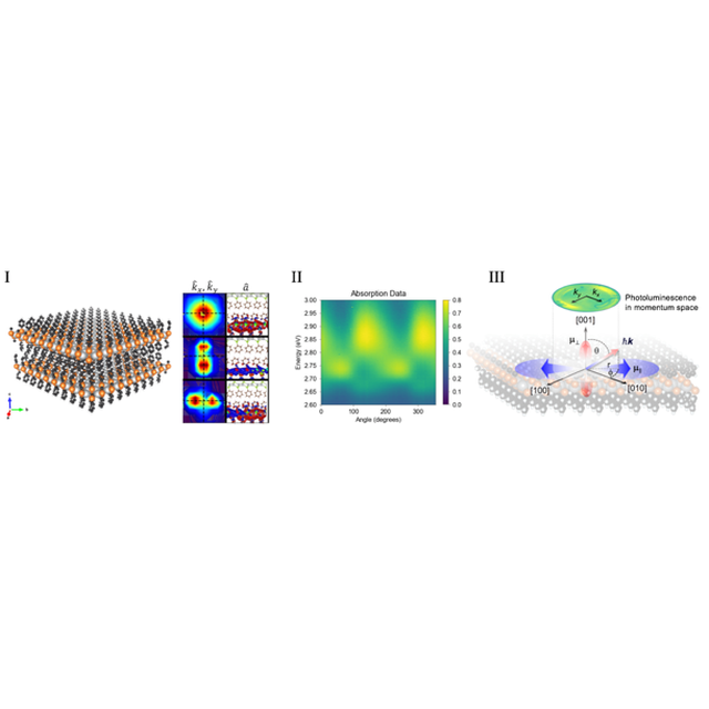
Theoretical and Experimental Observation of Anisotropic 2D Excitons in Self-Assembled Hybrid Quantum Wells
A009, C2N, PalaiseauSeminars
Self-assembled metal organic materials have great potential for optoelectronic applications due to their atomic and structural tunability. While a vast library of these materials has been studied, understanding optoelectronic properties to drive synthesis has been nearly impossible due to their complex structure. Here we consider the self-assembled layered bulk silver benzeneselenolate, [AgSePh]∞, as a representative of a class of coordination polymers exhibiting quantum well characteristics. Using ab initio density functional theory (DFT) and GW and Bethe-Salpeter equation (BSE) approach calculations, we predict and experimentally confirm two-dimensional (2D)-like excitonic and optoelectronic properties in the bulk phase arising from the quantum-confined charge carriers, including large exciton binding energies (~380 meV) and anisotropic absorption and emission. Our study demonstrates how integrating theory and experiment can elucidate general features in hybrid chalcogenide materials scalable via supramolecular chemistry with strong excitonic effects in the presence of anisotropic screening and strong confinement.
Figure 1. I, Material molecular representation with visualization of the predicted excitonic resonances. II, Experimentally measured strong absorption anisotropy. III, Experimentally observed anisotropic excitonic photoluminescence
Lorenzo Maserati Dr. Lorenzo Maserati graduated from Politecnico di Milano with a BSc (2007) and MSc (2009) in Physics Engineering. He obtained his PhD in Nanosciences from University of Genoa (IIT, 2014) with a thesis on colloidal nanocrystal films for optoelectronic applications. Then he joined the Lawrence Berkeley National Lab (LBNL) where he developed metal-organic frameworks membranes for gas separation. In a second postdoctoral appointment at LBNL, he focused his work on the excitonic properties of 2D and 2D-like materials, investigated by ultrafast spectroscopy. Dr. Maserati is currently Researcher at CNST (IIT) in Milan where he studies self-assembled metal-organic chalcogenides for optoelectronic applications. His interests range from materials chemistry to solid state and device physics. He is recipient of the “NanoInnovators’s got talent” award (Rome, 2016), and the Marie-Curie Seal of Excellence (2017).
Architecture and Decoration at the Nanoscale: programmable plasmonic and photonic thin film nanosystems through soft chemistry
Centre de Nanosciences et de Nanotechnologies, Amphithéatre, PalaiseauSeminars
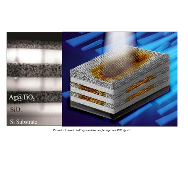
In the last years, soft chemical synthetic methods opened the path to create highly tunable thin film architectures, with complex yet controlled structure at different length scales. Optical nanosystems “decorated” with molecular, biological or nanoscale functions precisely located in space can be pre-designed and produced through the production and controlled assembly of nanobuilding blocks. In particular, Mesoporous Thin Films (MTF) are interesting for their tailorable optical, electronic or catalytic properties, and their compatibility with the requirements of electronics and optics industry. Each MTF is in turn a building block for more complex architectures with synergic properties derived from the control of the spatial location of well-controlled components.
We will present MTF architectures with programmable optical properties, in particular Mesoporous Photonic Crystals (MPC) and Nanoparticle-Mesoporous Nanocomposites (NMNC). These materials permit to harness and couple chemical and surface properties with photonic and plasmonic features of the ensemble. We can design and build stimuli-responsive autonomous systems that transduce chemical signals to optical response through information encoded in their structure at the molecular, mesoscopic or microscopic levels. The combination of the photonic and plasmonic properties of MPC and NMNC permits to exploit light confinement or amplification. These responsive nanosystems present applications in SERS, Tamm-based sensors, optical waveguides or photocatalysts.
Galo Soler-Illia studied Chemistry in the University of Buenos Aires, and performed a postdoc at UPMC, Paris. He is the Dean of Instituto de Nanosistemas at Universidad Nacional de San Martin, CONICET Principal Researcher, Associate Professor at the University of Buenos Aires, and Full Member of the National Academy of Exact and Natural Sciences of Argentina. He designs and produces intelligent nanosystems using chemical methods inspired by nature. He has published more than 160 papers in reviewed journals, with 13.000+ citations (h=45), and filed four patents.
Single molecule mechanics: gears, motors and cars
Centre de Nanosciences et de Nanotechnologies, Amphithéatre, PalaiseauSeminars
After the bronze Antikythera calculator (200 BC), the B. Pascal wooden calculating clock (1642 AC) and the micro-fabricated machineries on a silicon surface (middle of the 1980’s), it is now foreseen to miniaturise mechanical machineries down to the size of a single molecule.
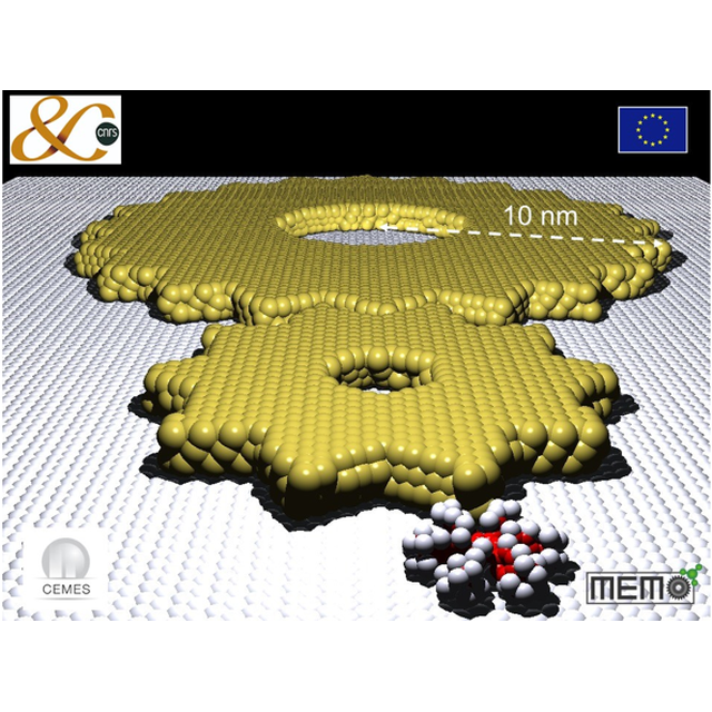
We will present our molecular design and experiments starting from the random rotation of a single molecule-wheel [1] and the step by step controlled rotation of a single molecule gear 1.2 nm in diameter [2]. More complex molecular machineries will be presented like a rack & pinion mechanism [3], a molecule wheelbarrow [4] and a train of molecule-gears. To drive molecule-machineries, we are using the mechanical interaction with the tip apex end atom of an STM and/or the inelastic tunnel current effect as exemplify with our step by step controlled molecule-rotor [5]. In the prospect to measure the motive power of a single molecule [6] and to interconnect mechanically a single molecule to the mesoscale, nano-fabrication of solid state nano-gears down to 30 nm in diameter will be presented [7]. We will end by a little survey of the April 2017 1st International Nanocar race [8,9] and by announcing Nanocar race II under the European project MEMO (Mechanics with Molecule(s)) for 2021.
References
[1] J.K. Gimsewski, C. Joachim, V. Langlais, H. Tang & J. Johanson, Science, 281, 531 (1998)
[2] C. Manzano, W.H. Soe, F. Ample, A. Gourdon & C. Joachim, Nature Mat., 8, 576 (2009)
[3] F. Chiaravalloti, A. Gourdon, C. Joachim & F. Moresco, Nature Mat.., 6, 30 (2007).
[4] C. Joachim, H. Tang, F. Moresco, G. Rapenne & G. Meyer, Nanotechnology,13, 330 (2002).
[5] U.G.E. Perera, F. Ample, H. Kersell, Y. Zhang, G. Vives, J. Echeverria, M. Grisolia,
G. Rapenne, C. Joachim and S.-W. Hla, Nature Nanotech., 8, 46 (2013).
[6] R. Ohmann, J. Meyer, A. Nickel, J. Echevaria, C. Joachim, F. Moresco and G. Cuniberti,
ACS Nano, 9, 8394 (2015)
[7] Deng Jie, C. Troadec, F. Ample & C. Joachim, Nanotechnology, 22, 275307 (2011).
[8] C.Joachim and G. Rapenne, ACS Nano, 7, 11 (2013).
[9] G. Rapenne and C.Joachim, Nature Rev. Mat. 2, 17040 (2017).
Opto-electro mechanics with photonic crystals
Centre de Nanosciences et de Nanotechnologies, Amphithéâtre, PalaiseauSeminars
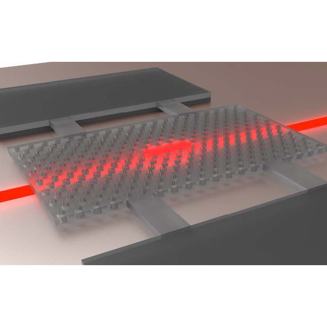
Optomechanics deals with the interaction of light with a mechanical oscillator. It utilizes the coupling between light and the geometry of a mechanical oscillator to read or tailor the mechanical motion of the resonator. This coupling is stronger at the nano-scale because of the very small mass of nano-mechanical resonator. We investigate the nano-optomechanics of suspended photonic crystal membranes. Depending on the arrangement of holes, the membrane can either act as a deformable end-mirror in a conventional Fabry-Perot cavity or include a cavity of diffraction-limited volume that simultaneously confines both phonons (i.e. mechanical vibrations) and photons. These structures combine cavity enhancement and low mass and thus exhibit strong mechanical coupling to light. In particular, optomechanical resonators formed by conventional photonic crystal membranes sustain mechanical modes ranging from the MHz to the GHz frequency. Depending on the configuration, photonic crystal membranes developed at C2N, allows studying nonlinear dynamics of single and coupled opto-electromechanical resonators, reaching microwave optomechanical oscillators and also temperature metrology.
Figure: Artistic view of radiation pression in bidimensional photonic crystal cavity em bedded in a suspended membrane.
Rémy BRAIVE is associate professor in Université de Paris and CNRS-C2N since 2009. After a PhD in “Optics and Nanophotonics” at University of Paris VII/LPN, he joined MPQ Garching (Germany) and then EPFL (Switzerland) as a post-doc where he started to get involved in the fields of nano-optomechanics. Since 2009, he carries his research activities at C2N where he launched a new direction line on optomechanics with suspended photonic crystal membranes https://toniq.c2n.universite-paris-saclay.fr/fr/membres/remy-braive/.
External visitors should be register
The human brain disconnectome
Centre de Nanosciences et de Nanotechnologies, Amphithéâtre, PalaiseauSeminars
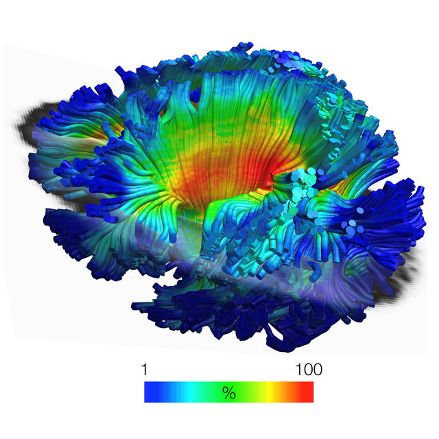
Patients with brain lesions provide a unique opportunity to understand the functioning of the human mind. However, even when focal, brain lesions have local and remote effects that impact functionally and structurally connected circuits. Similarly, function emerges from the interaction between brain areas rather than their sole activity. We will discuss a set of complementary solutions to measure the impact of a given lesion upon the neuronal circuits as well as ideas and theories explaining the functioning of the human brain.
Taken together, these neuroimaging measures will help discern the natural history of events occurring in the brain after a lesion, as well as assist in the localization of functions.
External visitors should be register beforehand (follow the link in the attached file)
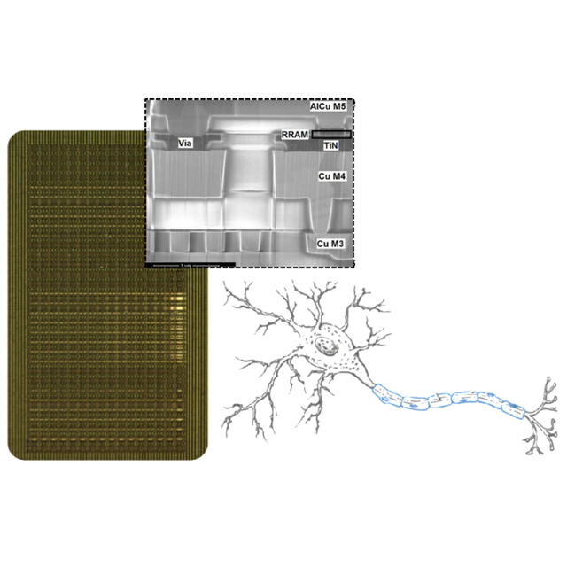
Neuroinspired Artificial Intelligence with Memory Nanodevices
Centre de Nanosciences et de Nanotechnologies, Amphithéâtre, PalaiseauSeminars
When performing artificial intelligence tasks, computers and graphics cards consume considerably more energy for moving data between logic and memory units than for doing actual arithmetic. Brains, by contrast, achieve vastly superior energy efficiency by fusing logic and memory entirely, performing a form of "in-memory" computing. Currently emerging memory nanodevices such as (mem)resistive, phase change and magnetic memories give us an opportunity to achieve similar tight integration between logic and memory.
In this talk, we will look at neuroscience inspiration to extract lessons on the design of such systems. We will first study the reliance of brains on approximate memory strategies, which can be reproduced for artificial intelligence. We will give the example of a hardware neural network relying on resistive memory. Based on measurements on a hybrid CMOS and resistive Hafnium oxide memory chip, we will see that such systems can exploit the properties of emerging memories without the need of error correcting codes, and achieve extremely high energy efficiency. Second, we will see that brains use the physics of their memory devices in a way that is much richer than only storage. This can inspire radical electronic designs, where memory devices become a core part of computing. We will illustrate this concept by our works using magnetic memories as artificial neurons. We have fabricated neural networks where magnetic memories used as nonlinear oscillators implement neurons, and their electrical couplings implement synapses. We will see that such designs can harness the rich physics and dynamics inherent to magnetic memories, without suffering from their drawbacks. This physics-rich approach nevertheless raises important challenges that we will highlight.
External visitors should be register beforehand (follow the link in the attached file)
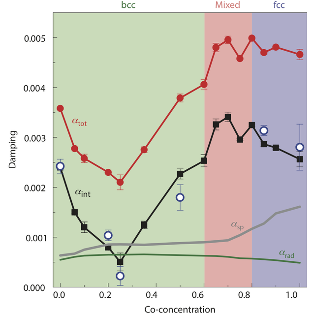
Broadband Ferromagnetic Resonance Spectroscopy: The “Swiss Army Knife” for Understanding Spin-Orbit Phenomena
Centre de Nanosciences et de Nanotechnologies, Amphithéâtre, PalaiseauSeminars
Modern spin-based technologies rely on multiple, simultaneous phenomena that originate from the spin-orbit interaction in magnetic systems. These include damping, magnetic anisotropy, orbital moments, and spin-orbit torques that are manifested in the spin-Hall and Rashba-Edelstein effects. While cavity based ferromagnetic resonance (FMR) spectroscopy has been used to characterize magnetic materials for many decades, recent advances in broadband and phase-sensitive FMR techniques have allowed further refinement, improved accuracy, and new measurement capability. In fact, broadband FMR techniques can now precisely measure spin-orbit torques at the thin-film level without the requirement of device fabrication.
Broadband FMR measurements have also improved our fundamental understanding of magnetic damping. Numerous extrinsic relaxation mechanisms can obscure the measurement of the intrinsic damping of a material. This created a challenge to our understanding of damping because experimental data were not always directly comparable to theory. As a result of the improved ability to quantify all of these relaxation mechanisms, many theoretical models have been refined. In fact, this has recently led to both the prediction and discovery of new materials with ultra-low magnetic damping that will be essential for future technologies based on spintronics, magnonics, spin-logic and high-frequency devices.
I will begin this lecture with a basic introduction to spin-orbit phenomena, followed by an overview of modern broadband FMR techniques and analysis methods. I will then discuss some recent successes in applying broadband FMR to improve our ability to control damping in metals and half-metals, quantify spin-orbit torques and spin-diffusion lengths in multilayers, and determine the interrelationships among damping, orbital moments, and magnetic anisotropy [4], [5]. The impact of these result on specific technologies will also be discussed.
Read more in the attached announcement.