
PhD defense
Monte Carlo simulations of phonon transport in nanostructures based on ab-initio methods
C2N - Centre de Nanosciences et de Nanotechnologies, , PalaiseauPhD defense
As the trend towards miniaturization of electronic devices continues, understanding heat transport at the nanoscale becomes increasingly crucial for developing energy-efficient and reliable systems. Conventional Fourier's law fails to capture the complex dynamics of phonon-based heat transport in such miniaturized devices. In this thesis, we study the phonon transport within nanostructures employing stochastic Monte Carlo methods. The accuracy of the simulations is enhanced by utilizing full band material description derived from ab-initio calculations based on density functional theory (DFT) without reliance on empirical parameters. We focus on examining alternative materials, such as GaAs, and 2D materials, like graphene, h-BN, and TMDCs, each selected for their unique thermal properties. This work not only offers substantial contributions to the field of thermal transport in nanostructures but also opens new pathways for the design and application of advanced materials in electronics.
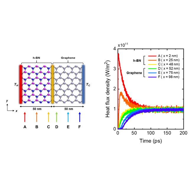
Figure :
- Left grahp : Sketch of the simulated 100 nm 2D h-BN/graphene lateral heterostructure with specific positions (A to F) marked for thermal transient analysis. Positions A, B, C, D, E, and F are located at 2, 25, 48, 52, 75, and 98 nm, respectively, along the x-axis within the structure. Red/blue faces for hot/cold thermostats with TH = 400 K, TC = 300 K, respectively.
- Right graph : Transient heat flux density at 6 points in 100 nm h-BN/graphene lateral heterostructure, measured from 0 to 200 ps. The rainbow color grade intuitively represents the varying heat flux densities according to their respective positions : red for position A, orange for B, yellow for C, green for D, blue for E, and navy for F.
C2N - Centre de Nanosciences et de Nanotechnologies, , Palaiseau
PhD defense
PhC nanolasers are receiving increasing attention due to their unique capacity to manipulate and confine light at a very small scale. Their small footprint and low thresholds make them ideal candidates for realizing optical interconnects, thus addressing the increasing demands for data transmission speed and power consumption. Moreover, their singular geometry enables the control of their spontaneous emission properties. This reveals the unique nature of PhC nanolasers from a fundamental perspective, highlighting their potential to serve as candidates for novel research in light-matter interaction. Despite these advantages, the current limitations in near-infrared detection capabilities impede the comprehensive characterization of their emission and dynamical properties, leaving a crucial gap in our understanding of these devices.
This thesis presents a time-gating detection technique based on four wave mixing, developed to measure the ultra-fast response of 1D nanolasers. By studying the interplay between nonlinearities and dispersion, a high sensitivity level of a few photons and a resolution of 2 picoseconds has been achieved. Further improvements in sensitivity, down to detection of less than one photon, are predicted by employing higher gate powers. This approach can be applied to the study of photon statistics and the quantum nature of materials.
The profiles of 1D nanolasers exhibit a rapid onset of emission and long decay, consistent with a β factor of 0.12 and a photon lifetime of 20 picoseconds.
A novel approach to obtaining the values of these two parameters controlling laser dynamics has been developed: they have been directly retrieved from the ultra-fast response of nanolasers, instead of solely relying on steady-state measurements such as the S curve, which, in many cases, can lead to inaccurate estimations due to the interdependence of these parameters. The dynamical response of 1D nanolasers is compatible with a maximum modulation speed of approximately 30 GHz, which fulfills the requirement for low-threshold ultracompact laser sources for photonic integrated circuits and optical communications.
The high sensitivity and resolution of the technique permitted the first measurement of an adiabatic wavelength conversion of photons with a wavelength shift as large as 1.2 nanometers. This demonstrates the potential of the technique in studying ultra-fast dynamics at near-infrared wavelengths.
Developing a slow-mode nanophotonic platform for strong interaction between cold Rb atoms and guided photons
C2N - Centre de Nanosciences et de Nanotechnologies, , PalaiseauPhD defense
Light-matter interaction at the single-quanta level is the keystone of quantum information science. However, single quanta are generally weakly interacting and enhancing this coupling has been the driving force for a large community and the development of the cavity quantum electrodynamics (CQED), where single atoms and single photons can be strongly coupled via a high-finesse cavity. Very recently, integrated photonic nanostructures appeared as a promising avenue of tailoring light-matter interaction by engineering the emitter environment. Modern nanofabrication techniques have enabled the design of solid-state systems with embedded emitters, such as quantum dots in photonic crystal waveguides or nanocavities with high-quality factors, leading to Quantum Nanophotonics. In this context, we explore the waveguide QED approach by trapping atoms close to photonic crystal waveguides exhibiting slowly propagating modes, reaching strong interaction without a cavity.
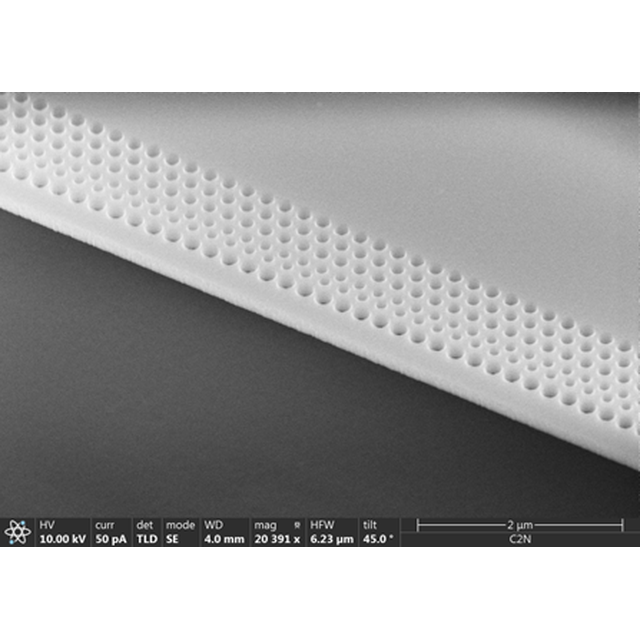
Figure : Suspended slow mode Half W1 photonic crystal waveguide fabricated in GaInP during the thesis.
(in french) Epitaxial growth by Molecular Beam Epitaxy of BiSb/MnGa Heterostructures for the charge-to-spin current conversion study
Auditorium de Thales R&T, , PalaiseauPhD defense
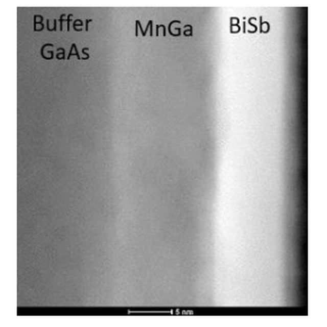
figure : STEM-HAADF cross section of the BiSb(9 nm)/MnGa(10 nm)//GaAs(001) heterostructure