With the perspective of studying the physical properties of novel two-dimensional materials, the MAT2D team at C2N has worked on the exploration of 2D quantum confined gaz in the 2H stacking of the α phase of In2Se3. The research team has identified this rather uncommon behavior for a ferroelectric material through ARPES measurements. These results were featured on the issue cover.
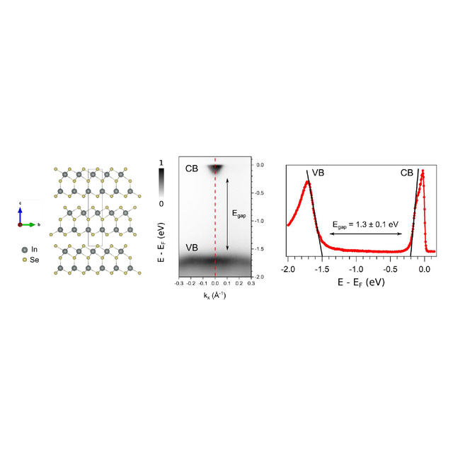
Ferroelectric-two-dimensional materials are promising compounds for next-generation nonvolatile memories, due to their low energy consumption and high endurance. The α phase of In2Se3 is one of the few 2D materials that fulfills all these criteria with both in-plane and out-of-plane ferroelectricity. This combination is a very promising and relatively uncommon behavior since most bulk ferroelectric materials gradually their ferroelectric character when thinned down to the atomic limit, due to the depolarization fields. Our team studied the structural and optical properties of α-In2Se3 as well as the electronic properties via angle-resolved photoemission spectroscopy (ARPES). Our findings unveil yet another unusual 2D phenomenon, related to the appearance of a highly metallic two-dimensional electron gas (2DEG) at the surface of vacuum-cleaved crystals. The presence of the 2DEG is also confirmed by thermoelectric measurements. In combination with DFT calculations, also performed C2N with the COMICS team, the experimental and calculated band structures reveal a direct band gap of energy equal to 1.3 eV, with the bottom of the conduction band localized at the center of the Brillouin zone, just below the Fermi level. The resulting strong n-type doping contributes to the formation of the observed 2DEG.
Reference :
Quantum Confinement and Electronic Structure at the Surface of van der Waals Ferroelectric α-In2Se3
Geoffroy Kremer1,2, Aymen Mahmoudi1, Adel M’Foukh1, Meryem Bouaziz1, Mehrdad Rahimi3, Maria Luisa Della Rocca3, Patrick Le Fèvre4, Jean-Francois Dayen5,6, François Bertran4, Sylvia Matzen1, Marco Pala1, Julien Chaste1, Fabrice Oehler1, and Abdelkarim Ouerghi1
ACS Nano 2023, 17, 19, 18924–18931
DOI : https://doi.org/10.1021/acsnano.3c04186
Affiliations
1Université Paris-Saclay, CNRS, Centre de Nanosciences et de Nanotechnologies, 91120, Palaiseau, France
2Institut Jean Lamour, UMR 7198, CNRS-Université de Lorraine, Campus ARTEM, 2 allée André Guinier, BP 50840, 54011 Nancy, France
3Université Paris Cité, Laboratoire Matériaux et Phénomènes Quantiques, CNRS, UMR 7162, 75013 Paris, France.
4SOLEIL Synchrotron, L’Orme des Merisiers, Départementale 128, F-91190 Saint-Aubin,
France
5Université de Strasbourg, IPCMS-CNRS UMR 7504, 23 Rue du Loess, 67034 Strasbourg, France
6Institut Universitaire de France, 1 rue Descartes, 75231 Paris cedex 05, France
Contact : abdelkarim.ouerghi@c2n.upsaclay.fr
Figure : Schematic representation of the side view of 2H α-In2Se3 and ARPES measurement of the valence and conductance bands enabling the experimental estimation of the gap value
Keywords : 2D materials, ferroelectricity, 2D electron gas, electronic band structure, photoemission spectroscopy, density functional theory calculations