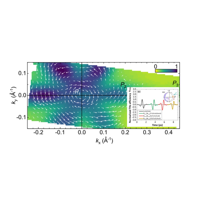
Quantum materials, and in particular topological insulators, offer new prospects for more efficient electronics that consume less energy. These materials, such as the Bi1-xSbx alloy, are insulators in depth but have spin-polarised conduction states on their surface. They enable a spin-charge interconversion that converts a population of spins from a ferromagnetic reservoir into a transverse charge current. In a recent work published in Advanced Science and resulting from collaboration between the Unité Mixte de Physique CNRS/Thales, LPENS, C2N and the SOLEIL synchrotron, we have measured helical spin-winding at the Fermi level using spin-angle resolved photoemission spectroscopy (SARPES) on the Cassiopeia light line of the Soleil synchrotron. We experimentally demonstrate the relationship between the spin and wave vector (k) of surface states in Bi1-xSbx, known as spin momentum locking. Secondly, using THz time emission spectroscopy, we demonstrate that this heterostructure enables efficient interconversion at the Bi1-xSbx/Co interface. This conversion emerges from the inverse Rashba-Edelstein effect up to a few nm from Bi1-xSbx. All the experimental data analysed using a strong bond model to calculate the electronic structure leads to the conclusion that the conversion effects linked to the particular spin nature of the surface electronic states at the Bi1-xSbx/Co interface are of interfacial origin. This work provides additional insight into the physics of inverse Rashba-Edelstein interface conversion in topological ferromagnetic/insulator heterostructures. In addition, this work opens up a new avenue in the field of THz emission with spintronic emitters.
Références
Spin-Momentum Locking and Ultrafast Spin-Charge Conversion in Ultrathin Epitaxial Bi1−xSbx Topological Insulator
E. Rongione1,2, L. Baringthon1,3,4, D. She1,3,4, G. Patriarche4, R. Lebrun1, A. Lemaître4, M. Morassi4, N. Reyren1, M. Micica1, J. Mangeney1, J. Tignon1, F. Bertran3, S. Dhillon1, P. Le Févre3, H. Jaffrès1, and J.-M. George1
Advanced Science, Volume 10, Issue 19, Jul 2023
DOI: 10.1002/advs.202301124
Affiliations
1Université Paris-Saclay, CNRS, Thales, Unité Mixte de Physique CNRS/Thales, F-91767 Palaiseau, France
2Laboratoire de Physique de l'Ecole Normale Supérieure, ENS, Université PSL, CNRS, Sorbonne Université, Universitè Paris Cité, F-75005 Paris, France
3Université Paris-Saclay, Synchrotron SOLEIL, L'Orme des Merisiers, Départementale 128, Saint-Aubin, F-91190 France
4Université Paris-Saclay, CNRS, Centre de Nanosciences et de Nanotechnologies, Palaiseau, F-91120 France
Figure : Color map representing the measured ARPES intensity (arb. units, proportional to the DOS at the Fermi level) closeto Fermi energy integrated on 25 meV with arrows representing the measured spin polarization direction and amplitude (T=300 K). The differentelectron and hole pockets labeledP1,P2,andP3in (d) are easily identified in the experimental measurements. The value of the colorbar indicates thefull range (0–1) between 0 and the maximum value ofP(0.5±0.2).